Analyzing RF architecture performance up front
Next-generation communication design demands ever-more-innovative RF technologies
BY JOEL KIRSHMAN
Applied Wave Research
El Segundo, CA
http://www.appwave.com
Wireless communications are rapidly evolving in both commercial and defense marketplaces. Whether it’s a commercial WiMAX or a military satellite communications application, RF system/subsystem designers are under constant pressure to improve data throughput.
The ability to gain the best understanding of the radio design as early in the design process as possible enables these design teams to meet their throughput challenges. The sooner designs can be perfected and performance tuned and optimized, the greater the chances for success—a quality product introduced into the market before the competition.
Spreadsheets
A disappointing truth, however, is that many software tools have not kept pace with engineers’ needs. As a result, designers often rely on spreadsheets to obtain a first-hand analysis of system-level performance. While a spreadsheet is better than no tool at all, it fails to give an in-depth analysis of the performance of an RF link.
Additionally, spreadsheets neglect to account for component mismatch or to allow for the importing of circuit designs or S-parameter data files. Spreadsheets also lack a GUI and a host of other RF/system aware-features like ready-selectable RF components, a spectrum display, and the capability to identify causes of spurs or intermodulation products.
Furthermore, using a spreadsheet consumes significant time as the user self-perfects the macros that need to be developed and optimized for each and every design variation or new design. This spreadsheet design methodology also introduces errors downstream because users of the spreadsheet and/or its results can be unaware of the assumptions/caveats contained within it, and can unknowingly forward-propagate erroneous data and/or specifications. The result of such a flow is that multiple iterations of a design are actually bread-boarded and tested several times over before specifications are solidified. Any costs saved through the use of a spreadsheet early on are later squandered in hours of laboratory testing and design respins.
The need for new tools
In order to meet today’s requirement to deliver quality, high-performance products to market ahead of schedule, a better solution for the upfront analysis of RF architecture performance is necessary. While it may be hard to break away from the familiar spreadsheet flow, what is gained is that the back-end process of bread-boarding and testing in the laboratory are eliminated, saving valuable man-hours, hardware dollars, and design turns.
New EDA software is being developed to streamline the RF system design process and provide for the planning and analysis of RF architecture performance. Applied Wave Research for example, has developed the RFA advanced system-level planning and specification tool to help RF engineers explore design options early and gain insight into their designs from day one.
This and other new EDA technologies enable communications designers to streamline their product development process and reduce, if not eliminate, their dependencies on spreadsheets and bread-boards.
Two key technologies for RF system design are as follows:
• RF budget (RFB) analysis. Enables designers to make traditional RF cascaded measurements such as gain, noise figure, and third-order intercept, inclusive of image noise and mismatch, along a communication link. Provides engineering teams with an efficient means to prevent the over specification of components and thereby reduces costs.
• RF inspector (RFI) technology. Enables designers to identify the cause or heritage of any intermodulation product or spur of an RF link. Allows users to readily isolate the sources of unwanted interferers, and therefore better architect the RF system.
This article discusses these enabling technologies in the context of an RF system design. With reference to RFB, the design displayed in Fig. 1 is an RF link with an automatic gain control (AGC) loop.
The RF link consists of two amplifiers, a filter (realized by Touchstone data), and a variable gain amplifier (VGA). The amplifier model is, in fact, dependent on a data file (format shown in Table 1 ) that accounts for the frequency dependency of common amplifier parameters inclusive of input and output reflection coefficients. The VGA accounts for frequency dependency, hysteresis, and S parameters.
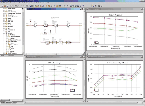
Fig. 1. The above is an RF link with AGC loop.
In both cases, the frequency-dependent settings are interpolated for frequencies between the smallest and largest frequencies. The models also incorporate saturation shaping of the input signal. For engineers who want to work at the highest level of abstraction, RF models with parameter windows for P1dB, IP3, NF, gain conversion, etc. also exist.
Table 1. Amplifier Data File
| FRQ (GHz) | Gain (dB) | OP1 dB (dBm) | OIP3 (dBm) | NF (dB) | S11 (Mag) | S11 (Phs, deg) |
| 0 | 10 | 20 | 30 | 2 | 0.7 | 30 |
| 0.5 | 16 | 25 | 34 | 3 | 0.7 | 32 |
| 1 | 19 | 30 | 42 | 3.5 | 0.78 | 35 |
The simulation is set to sweep through several frequency points and power levels. For each frequency the cascaded noise figure (NF), gain, and output power vs. input is monitored. For example, in the case of the NF vs. frequency graph, each input power level is represented by a different color trace and the x axis is defined as frequency.
The power-in vs. power-out graph shows the region of operation for relatively stable gain. Thus, from an RF subsystem designer’s point of view, a very powerful tool that surpasses the capability of a spreadsheet can be used to gain a qualitative feel of the AGC loop under realistic conditions all in the matter of eight mouse clicks and under 5 min from start to finish.
Clearly, the graphical interface, inclusive of both optimization and yield analysis reveals the advantages of an EDA system simulation tool to a spread sheet, not only in the ease-of-use and quick learning curve provided by the graphical user interface (GUI), but also in accurately accounting for real-world circuit interactions. Setting up the simulation takes several minutes and once you do, it is ready to be invoked instantly for the next design or variation.
In switching technologies now to the RFI, it helps to think of RFI as a system-level frequency-domain circuit simulator. It solves for voltages and currents at each RF node for each generated spectral component. RFI includes the effects of conversions, harmonics, inter-modulation and mixer leakage (for example, LO-to-IF, IF-to-RF and RF-to-IF). In addition, one can either stimulate the RF link with continuous wave (CW) signals and/or modulated signals.
| Table 2. Choices available for employing RFI technology after down-converting a signal |
| Use RFI to: • Determine the various contributors to the frequency content. • Identify the path of the contributors. • Examine the voltage, current and power of each contributor. • Classify the contributors as signal of interest, distortion, or interference. |
Table 2 shows the choices available for employing the RFI technology. In terms of viewing the spectrum, the user can either monitor the full spectrum, the spectrum of just the signal, or spectrum of the distortion products. Designers can take advantage of the dynamic M probe and monitor the spectral content of any node post simulation; hence they are not required to start another simulation if they decide to monitor the output of another node.
Additionally, the RFI software interface provides a clean and efficient means of determining the individual contributions to a particular tone. Users can simply double click on a tone to open up the RFI dialog box, which contains detailed information about the content of the selected spectrum component. Flags of different colors are used to easily enable users to identify the desired signal, intermodulation products, and distortion products.
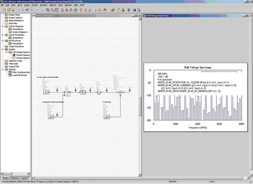
Fig 2. RFI is used to identify the cause of a spur.
Ultimately, RFB and RFI are indispensable tools for RF communication system engineers who need to quickly create and verify the initial specifications of a radio design before committing to hardware and/or a particular circuit design. In other words, it’s a virtual sandbox from which to experiment with various communication standards so that the best design decisions can be made as soon as possible. ■
For more on RF ICs, visit http://electronicproducts-com-develop.go-vip.net/linear.asp.
Advertisement
Learn more about Applied Wave Research


