By Jean-Jacques DeLisle, contributing writer
A new light-emitting device has been developed in the laboratory of Ali Javey, professor of electrical engineering and computer sciences at Berkeley, and it may have a very bright future. The new device is three atoms thick and can be made smaller than a human hair. Funded by the National Science Foundation and the Department of Energy, the advancement was published in Nature Communications on March 26. A previously published work by the Ali Javey lab in 2015 showed how different semiconductors were capable of emitting light, but they were unable to create a functioning light-emitting device.

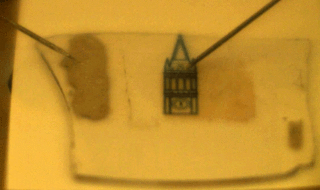
The atomically thin light-emitting device opens the possibility for invisible displays. Image source: Berkeley.
The new report published in Nature Communications shows proof of concept for a new type of LED that can overcome some of the fundamental problems with LED technology today. In traditional LEDs, an electrical current is passed through the light-emitting diode and creates light using a DC current. These are efficient but not as scalable as modern tech companies would like. The new LEDs are much smaller than their predecessors, and according to its creators, it can even be made invisible..
“The materials are so thin and flexible that the device can be made transparent and can conform to curved surfaces,” said Der-Hsien Lien, a postdoctoral fellow at UC Berkeley, in a press release. Der-Hsien Lien is a co-first author along with Matin Amani and Sujay Desai, doctoral students in the Department of Electrical Engineering and Computer Sciences at Berkeley.
The new LEDs function on an AC field, unlike previous LED technology that required current injection. The field results from an AC voltage connection to the LED monolayer and to an insulator underneath the monolayer, so there is only one point of contact to the LED itself rather than the two points that are required for typical LEDs. This cuts down on material cost and allows the devices to be miniaturized. The devices work by laying the semiconductor monolayer on an insulator and placing electrodes on the monolayer and underneath the insulator. In this arrangement, researchers could apply an AC signal across the insulator and excite the semiconductor, creating light.
The applications for this new technology are wide-ranging. Powerful lights could be invisibly installed for security systems. Tiny transparent displays could disappear and reappear as they are needed or be used on windows on skyscrapers that softly glow at night, reducing energy costs. The devices could even be embedded under the skin to create glowing tattoos. The technology shows a lot of promise, though it is still in its fledgling stages. “A lot of work remains to be done and a number of challenges need to be overcome to further advance the technology for practical applications,” said Javey. “However, this is one step forward by presenting a device architecture for easy injection of both charges into monolayer semiconductors.”
Advertisement
Learn more about Electronic Products Magazine


