Autocalibration solutions for optoelectronic switches
Compensating for manufacturing variations, temperature changes, and LED degradation boosts reliability and life expectancy
BY BOB PROCSAL
OPTEK Technology, Carrollton, TX
http://www.optekinc.com
Taking the product variances out of your optoelectronics designs has the potential to dramatically improve the reliability, performance, and life expectancy of the equipment in which they are used. Ideal optoelectronic manufacturing would have a 2:1 variance in the minimum to maximum output of a device, but today’s optoelectronic manufacturing process operations cannot economically achieve this precise control in producing devices. Therefore the designer must take into consideration all possible product variations, including min / max electrical characteristics, as well as performance changes over time and temperature.
Operation and variations
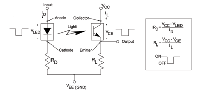
Optical switching occurs when the LED radiates light on the phototransistor and a current begins to flow. This load current (IL ) can be changed to a voltage and easily measured by adding a resistor (RL ) to either the collector or emitter (see Fig. 1 ).

Fig. 1. Resitors RD and RL control current in the switch’s LED and photoresistor, respectively.
The LED’s forward, or drive, current (ID ) is used to control the amount of light being radiated. This current, which is controlled using a limiting resistor (RD ), typically ranges from 5 to 20 mA. The values of both RD and RL can be calculated using relatively simple equations. Typical values are in the 10-kΩ range.
As mentioned, manufacturing variances in the devices themselves can create output current variations. Slotted or reflective switches are built with an LED and photosensor (photodiode, phototransistor, or Photologic) and are tested and categorized into groups. These subsequent groupings provide the desired input and output electrical characteristics.
Typical variation for the electrical output IC(ON) has a ratio (maximum IL / minimum IL ) from 3 to 7. (For example, if IL maximum is 5 mA and IL minimum is 1 mA, the ratio is 5 / 1, or simply 5.) The design engineer must take these variations into consideration during the equipment design cycle.
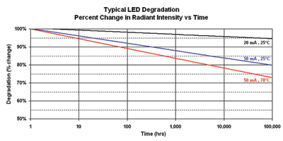
Another design consideration is inherent degradation of the LED. As LEDs age, they all have a tendency to lose efficiency with respect to optical power. Typical degradation is referenced at 25°C with a known LED current (ID , typically 20 mA).
As shown in Fig. 2 , the output typically degrades between 5% and 20% over 100,000 hours or 11.4 years. This might seem to be a long time, but a lot of equipment is expected to operate for more than 10 years, thus the design engineer needs to take this into consideration.

Fig. 2. With age, LED output decreases for the same current input.
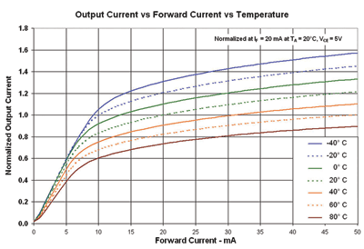
In addition to manufacturing variation and LED degradation, the ultimate use for the application must also be taken into consideration. Temperature changes can have a significant affect, affecting both the amount of light emitted by the LED as well as the sensitivity of the photosensor. The fact that, when temperature increases, the light emitted by the LED decreases while the sensitivity of the phototransistor increases helps offset problems, but it doesn’t totally fix them.
For a typical LED and phototransistor, the actual amount of change in output current versus temperature may increase or decrease, depending on the characteristics of the LED and phototransistor (see Fig. 3 ). For those applications where temperature variation is a design factor, this must also be considered.

Fig. 3. As temperature increases, the output of a phototransistor can decrease significantly.
Variation in the power supply may also occur. As the power source varies due to temperature, load, and aging factors, the drive current for the LED may change, as may the output current of the phototransistor. Power-supply-related variation is typically small (unless the power source is on the verge of failure), and designers can expect a 0% to 2% change.
Compensating for variations
So now we know that an optical switch has an LED and photosensor that can have an output current maximum / minimum ratio in the 3 to 7 range at room temperature. Adding LED degradation at 5% changes this ratio to 3.15 to 7.35 and with –40° to 85°C temperature variation, the ratio is 5.53 to 12.90 or more.
For simple optoswitch designs, ensuring the minimum amount of output current becomes the most important design factor. To do this, one must take into consideration the specified electrical characteristic variation, temperature fluctuation, LED degradation and finally the change in the power source. Designing with these characteristics in mind provides a more robust and stable solution.
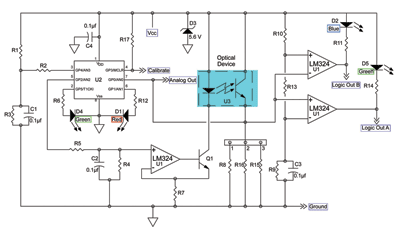
What is needed is circuitry that would allow the system to be calibrated at any time. By providing the flexibility to calibrate before or after being assembled in the equipment, the circuit can compensate for degradation of the LED’s output over time and thus extend its life. Further, the circuit could store calibration settings and set-up information. A circuit capable of just such performance is shown in Fig. 4 .

Fig. 4. This circuit can automatically recalibrate a sensor over its lifetime.
Momentarily grounding the circuit’s “calibrate” pin allows the programmed routine stored in a PIC microcontroller (U2) to begin automatic calibration. This can be done at any time during a product’s life, extending the sensor’s LED life by compensating for degradation. A technician would be able to recalibrate a customer’s sensors remotely to correct a performance problem caused by any of the mentioned variances.
The auto-calibration circuit is designed to compensate for optical-device changes due to manufacturing variance. It could be used to calibrate either reflective or interruptive devices, thereby providing a consistent output and eliminating the requirement to confirm either the LED drive resistance or phototransistor load resistor to maintain a consistent output steady-state condition.
The design engineer can narrow the expected startup output state while providing a device that operates with that startup state for years, thus enhancing system reliability and consistency. Degradation of the LED or phototransistor is compensated for each time the system is calibrated. The circuit could maintain the calibrated setting even if power is lost, allowing faster startup.
The circuit has a set of shorting pins that allow the user to change the phototransistor’s load resistor, R8 , R16 , and R15 . By arranging the shorting bar to the appropriate location, the load resistance could be changed from approximately 2.5, 9.6, or 27 kΩ, increasing the sensitivity of the device.
When the “calibrate” pin is momentarily grounded, the circuit begins its calibration process by raising the current through the LED from 0 to 14 mA, until the phototransistor reaches a preset output level, causing a green calibration light to blink three times. The LED drive current is locked and maintained until the Reset/Clear pin is grounded. If the LED drive current reaches the maximum allowable value, a red warning light can be programmed to turn on. During this calibration process, remote monitoring of the “analog out” pin would allow the designer to ensure the system is calibrated (a nominal setting for this preset calibrated output level is ½ VCC , when the calibration procedure is completed). The phototransistor’s load resistor may need adjustment for the system to calibrate properly.
The “analog out” pin lets the design engineer set any reference point to recognize an optical change for the device being monitored. The logic output pins will change state once the preset optical light condition is reached. The values of resistors R10 , R13 , and R9 set the condition. The “Logic Out A” pin switches state when the optical signal increases above approximately two-thirds of VCC while “logic out B” switches state when the optical signal decreases below about 1/3 of VCC .
A preconfigured version of this circuit is available on a pc board, as part of the OCB100-Kit auto-calibration design kit. The kit also provides a number of different types of sensors for use in setting up the circuit for a particular app. ■
Advertisement
Learn more about TT electronics Optoelectronics Business Unit (OPTEK)


