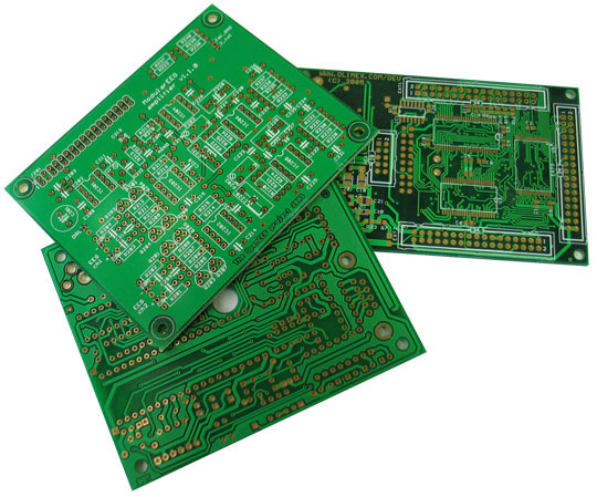
The Printed Circuit Board (PCB) is what connects and holds together all electronic components. Designing electronics is very complex, but we’ve put together the most common mistakes to avoid that often occur on the PCB.
High-current traces that aren’t wide enough
If a PCB trace needs to handle current greater than a few hundred milliamps, the minimum width most likely won’t be enough. A trace on an external layer carries more than an internal trace for the same thickness. The reason for this is because the external trace has superior air flow and heat dissipation.
Copper weight measures the thickness of copper used on each trace. Most PCB manufacturers allow users to choose from weights of 0.5 oz./sq. ft. to 2.5 oz./sq. ft. For a proper calculation, use a trace width calculator, specifying the permissible temperature rise, in order to compute its current carrying capacity. A standard choice is a 10°C rise, but for those who need a narrower trace width, you can use a 20°C or higher temperature rise.
Errors in landing patterns
Design software packages provide libraries of electronic components, of which include the schematic symbol and PCB landing pattern for each. Traditionally, you won’t have any issues if you stick to these components in your design. However, if you use any outside of these libraries, then you must manually draw the schematic symbol and the PCB landing pattern. Be sure the pad-to-pad spacing isn’t off even by a fraction of a millimeter, because then the pins won’t align properly, making soldering near impossible.
Incorrect antenna layout on wireless designs
For products that use wireless technology, the layout of the antenna on the PCB is vital. To achieve a maximum power transfer between the transceiver and the antenna, users must match the complex impedance, not the simple resistance. You will need a proper transmission line to connect the antenna and the transceiver. Often, the transmission line should have 50-ohm impedance for maximum power transfer with the antenna.
To find the PCB transmission line dimensions used to achieve proper impedance, you can take advantage of a unique calculator, such as the free AppCad from Avago. Typically, a matching circuit, such as an LC pi-network, is required between the antenna and the transceiver, allowing you to fine-tune the impedance.
Decoupling capacitors not used or improperly placed
Components in a design need a stable voltage. To help serve this function, users should decouple capacitors on the power supply rail. Do note: decoupling power capacitors need to be as close to the pin as possible to ensure a stable voltage. Additionally, the power trace from the supply rail needs to go through the decoupling capacitor before it reaches the pin that requires the stable voltage.
For highly sensitive components, such as analog-to-digital converters, a series inductor should be added, creating a low-pass LC filter to remove any supply noise.
The layout of switching regulators should not be optimized
There are two types of voltage regulators in electronic designs: a linear regulator and a switching regulator. The linear regulator typically wastes a substantial amount of power, but they’re often inexpensive and easy to lay out correctly. However, for high-power or ultra-low-noise applications, the design for a linear regulator is more critical.
While switching regulators are more complex, they are much more efficient. The less power that is wasted, the longer the battery life is. Do note that they require a more careful layout on the PCB, so datasheet guidelines need to be followed carefully.
Avoid blind/buried VIAs that are used or non-manufacturable
A VIA hole passes through all layers of the board. The major issue with this is that it can increase the size of the PCB because the VIA reduces routing space on every layer.
A blind VIA connects an external layer to an internal layer, and a buried VIA connects two internal layers. But, it’s not that simple. Blind and buried VIAs have huge limitations based on how the layers stack up on the board. Additionally, they drastically increase prototyping costs, which is why they’re not recommended for most applications.
High-speed traces that are too long
As a general rule of thumb, high-speed signals should follow the shortest, straightest path possible. For many designs, this refers to the routing of any high-frequency crystals.
Most microcontroller-based designs require few super-high-speed signals. But if your product uses a high-speed microprocessor with external data and address bus, then the trace path is notably more important.
Source: Makezine
Advertisement
Learn more about Electronic Products Magazine


