The challenge for a low-power LED design is to keep power conditioning, conversion, and load control in balance
BY ALEXANDER CRAIG
Principal Engineer
Fairchild Semiconductor
www.fairchildsemi.com
Low-power LED solutions typically consist of a single string of LEDs or a single input and output control point for the LED driver. These drivers must perform the basic functions of any LED power supply, such as power conditioning and conversion and load control. High-power solutions can often leverage specialist stages for these functions. Low-power solutions of less than 35 W, such as a light bulb, must perform all three functions in as few stages as possible, because cost and space are at a premium.
The challenge for a low-power LED design is to achieve a balance of power conditioning set by regulatory standards. Power conversion, also guided by regulatory standards, must be safe and efficient. Superior load control must be incorporated. This includes constant current regulation and dimming fidelity, which is generally set by market acceptance. The FL7730 and FL7732 PFC controllers strike this balance quite well and perform all three functions in one stage. With these solutions there is significant interplay among all three functions. To understand the solutions we will start with the highest order and focus primarily on power conditioning and power conversion. The interplay of load control does take part in power conditioning, but in order to meet power conditioning standards and market requirements, understanding how to achieve power condition, such as EMI requirements and power factor, is vital. The next step is to understand load control, such as fault protection, constant current control and dimming.
Flybacks are used for most low-power isolated LED supplies, but not all flybacks are alike. The operation and regulation of a flyback will affect system performance and cost. The typical flyback used for low-power supplies is not power factor corrected and tends to have a high-voltage electrolytic capacitor after the bridge rectifier.
These supplies are typically secondary side regulated (SSR), meaning they have an optocoupler, a voltage reference and a fast loop band width of 1 kHz to react to load charges. This type of flyback is not ideal for LED lighting for two reasons: the flyback is not power factor corrected and is typically set up as a constant voltage supply where LEDs are better driven with content current.
In single-stage flyback PFC, quality power factor is achieved by using a boundary, or critical, conduction mode PFC control IC that uses a fixed on-time variable switching frequency scheme. This feature improves and maintains the power factor but places restrictions on the turns ratio “n” and output voltage of the transformer where n = VRO /VO + VF . Equation 1 shows the input current as a function on phase angle. The denominator makes the current shape non-sinusoidal, unless the ratio VIN Peak /VR is made very small where VR is the reflected voltage.
Equation 1

With higher reflected voltages required to achieve an expectable power factor, the stress on the MOSFET voltage can be increased where VDS,max = VIN,PK,max + VR + Vspike . These restrictions tend to force the use of higher-voltage MOSFETs: ~800 or 900 V.
This approach typically uses a SSR constant current control scheme that measures the load current and voltage directly. Power loss is incurred in measuring the load current but good constant-current control of a few percent can be achieved but an optocoupler is also required. These supplies operate with a slow feedback loop of ~20 Hz, which works well for LED loads because they are not dynamic. The energy storage performed by the high-voltage electrolytic capacitor in the classic flyback is accomplished with lower-voltage (LED string voltage) capacitors.
To work around cost limitations with the single-stage flyback PFC, some have tried a primary side regulated (PSR) flyback with a passive PFC. This approach reduces the power loss on the SSR and the voltage stress on the MOSFET, however this process uses HV capacitors and other parts in the primary side which limits power factor, lifetime, and size.
To achieve a cost effective balance of power conditioning, power conversion and load control for LED applications a new approach is employed with the FL7730 and FL7732. These PWM controllers uses a different type of single-stage topology with primary side regulation, allowing isolated LED drivers to be created with fewer components and minimized cost without requiring a high-voltage input capacitor or SSR feedback circuitry. Refer to Fig. 1 for the simplified overall schematic.
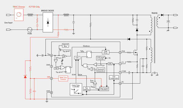
Fig. 1: PWM controller schematic with primary side regulation, allowing isolated LED drivers to be created with fewer components.
To achieve good power factor and low THD, the flyback is operated in DCM at a fixed frequency with constant on-time over the half sine wave. Therefore the input current is
IIN = IP_avg = TON (VIN /Lm )TON / 2T and is proportional to VIN . With this approach good power factor does not require a high reflected voltage, thus allowing the use of less expensive 600-V MOSFETs in place of costly 800- or 900-V MOSFETs.
The center peace of the FL7730 and FL7732 is the PSR Load control function block. This unique circuitry is called the TRUECURRENT control and has been proven in applications such as chargers. By adding two key features to the TRUECURRENT control the FL7732 and FL7730 can accurately regulate output current versus changes in input voltage, output voltage and magnetizing inductance variation. For FL7730 designs, the device also allows for a simple but effective dimming.
The basic operation of the TRUECURRENT control block is illustrated in Fig. 2 and Eq 2 .
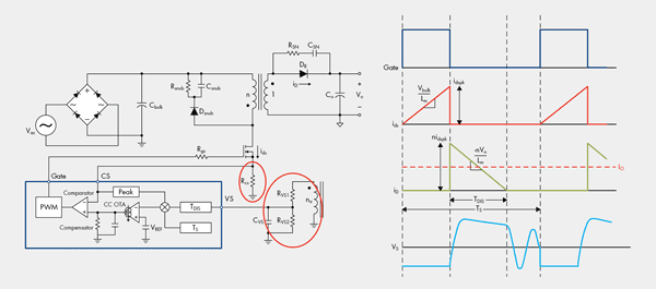
Fig. 2: The TRUECURRENT PSR Load control function block can regulate output current versus changes in input voltage, output voltage, and magnetizing inductance variation.
Equation 2
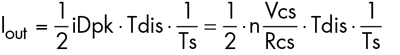
Equation 2 describes how the output current is determined by the diode peak current and the discharge time on the energy stored in the transformer. The output current (IOUT ), the average of the diode current in steady state, is estimated using the peak inductor current as measured by the current sense resistor at the source of the MOSFET and inductor current discharge time (Tdis ) as measured by the VS pin shown in Fig. 1. Since the output current (IOUT ) is the average of the diode current in steady state. Proper selection of the current sense resistor (RCS ) allows the measurement of the peak drain current value with a peak detection circuit. The IOUT is calculated using the inductor discharge time and can be measured in the VS pin. When the diode current goes to zero, the voltage on the VS pin starts to rapidly decrease as can be seen in Fig. 1. These measurements and the knowledge of the switching period (TS ) are the primary factors on the TRUECURRENT control block.
This output information is compared with a precise internal reference to generate an error voltage (VCOMI), which determines the duty cycle of the MOSFET (Q1 ) for constant-current-mode operation. This innovative technique is how the FL7732 and FL7730 precisely control a constant-current output. This can be seen in Fig. 3 and Table 1 , which show measured results from an evaluation board showing constant-current deviation in the wide output voltage range from 11 to 28 V of less than 2.1% at each line-input voltage.
The first key feature added for lighting is the Line Compensator that receives information about the line voltage from the VS pin and uses it to modify the peak current circuit. This innovative solution allows for extremely tight tolerances and constant-current regulation over a wide input voltage range. This can be seen in Fig. 3 and Table 2 , which show measured results from an evaluation board showing constant-current deviation in the wide line regulation at the rated output voltage (24 V) is
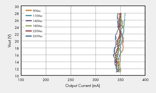
Fig. 3: Constant-current regulation showing measured results from an evaluation board.
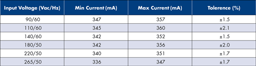
Table 1: Constant current regulation by line voltage change (11 ~ 28 V)
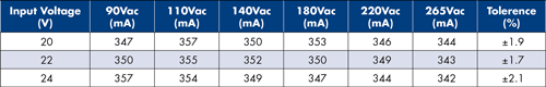
Table 2: Constant current regulation by output voltage change (90 ~ 265 Vac)
A more detailed explanation of the operation of high power factor PSR flyback can be found at www.fairchildsemi.com/an/AN/AN-9750.pdf.
The second key feature for lighting is the dimming control function, which will be explained in more detail in a future article. ■
Advertisement
Learn more about Fairchild Semiconductor


