By Majeed Ahmad, contributing writer
Cameras have revolutionized smartphones, cars, surveillance, and gizmos offering augmented reality (AR) and virtual reality (VR) functions. Now, 3D sensors are taking this imaging revolution to the next level by simultaneously detecting and classifying a variety of objects in real time.
Apple’s iPhone X incorporating 3D facial recognition instead of a fingerprint sensor or PIN is a case in point. The trendsetting handset is now eyeing to take the 3D-sensing–enabled facial recognition to secure biometrics for mobile payments, gesture sensing, and immersive shopping and gaming experiences.
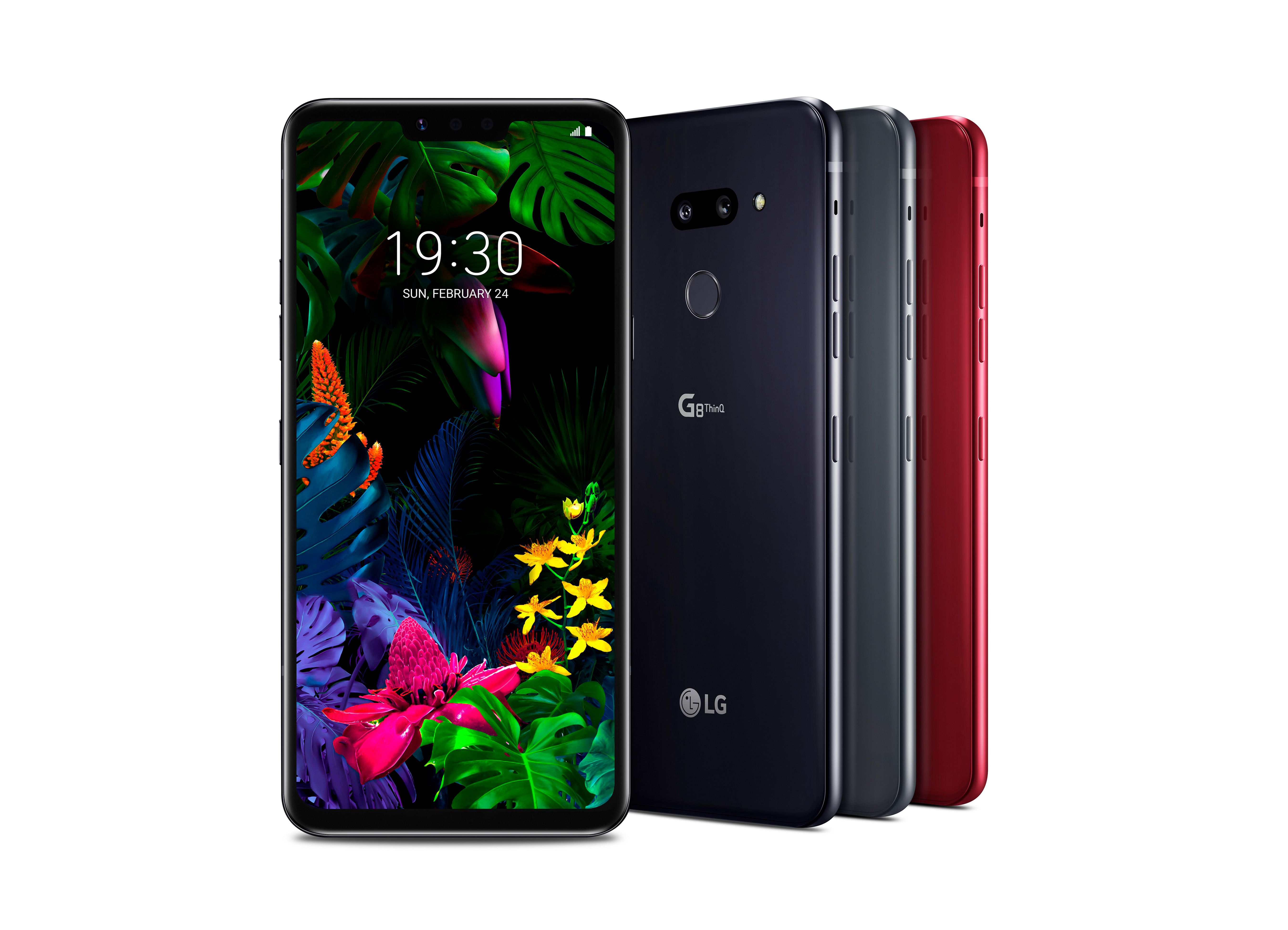
Infineon’s REAL3 image sensor enables gesture recognition in LG’s G8 ThinQ smartphone. (Image: Infineon)
It’s worth mentioning that 3D sensing first emerged in data communications during the mid-1990s in the form of vertical-cavity surface-emitting laser (VCSEL) technology. Fast-forward to 2017: Apple brought 3D sensing to the consumer realm when it integrated three different VCSEL dies in the iPhone X for the proximity sensor and the Face ID module for accurate facial recognition.
Android phone makers are following suit with 3D sensing adoption, while sensor suppliers like ams are starting to release VCSEL chips to power the front- and rear-facing 3D cameras. These smartphones will be able to accurately calculate depth in a room, identify gestures in virtual games, and display virtual characters in front of and behind real-life objects.
According to market research firm Gartner Inc., by 2021, nearly 40% of smartphones will be equipped with 3D cameras. These 3D-sensor–enabled smartphones will play a vital role in facilitating the next-generation interactive visual experiences like AR functions.
But while smartphones are accelerating the development and commercialization of high-precision 3D sensing, we also see the adoption of 3D-sensing–based camera systems in a wide array of segments ranging from automotive to industrial to surveillance.
3D sensor basics
A 3D sensor differentiates between objects, determines location while mapping large areas, and creates a detailed image of an object or environment. That makes 3D-sensing camera solutions a key ingredient in scanning, depth-sensing, and facial-recognition applications.
There are two primary technologies used to capture and present the information in 3D formats: structured light and time of flight (ToF). A structured-light sensing system projects an active pattern of dots and obtains depth by analyzing the deformation of this pattern. The first-generation Kinect, for instance, used a structured-light camera.
ToF, probably the most widely used technology in 3D sensors, sends out invisible laser pulses and measures how long they take to bounce back. The second-generation Kinect employed a ToF camera. The ToF sensors are gaining traction because they enable device miniaturization and energy efficiency. On the other hand, structured-light sensors can provide higher-resolution mapping at a reasonable cost.
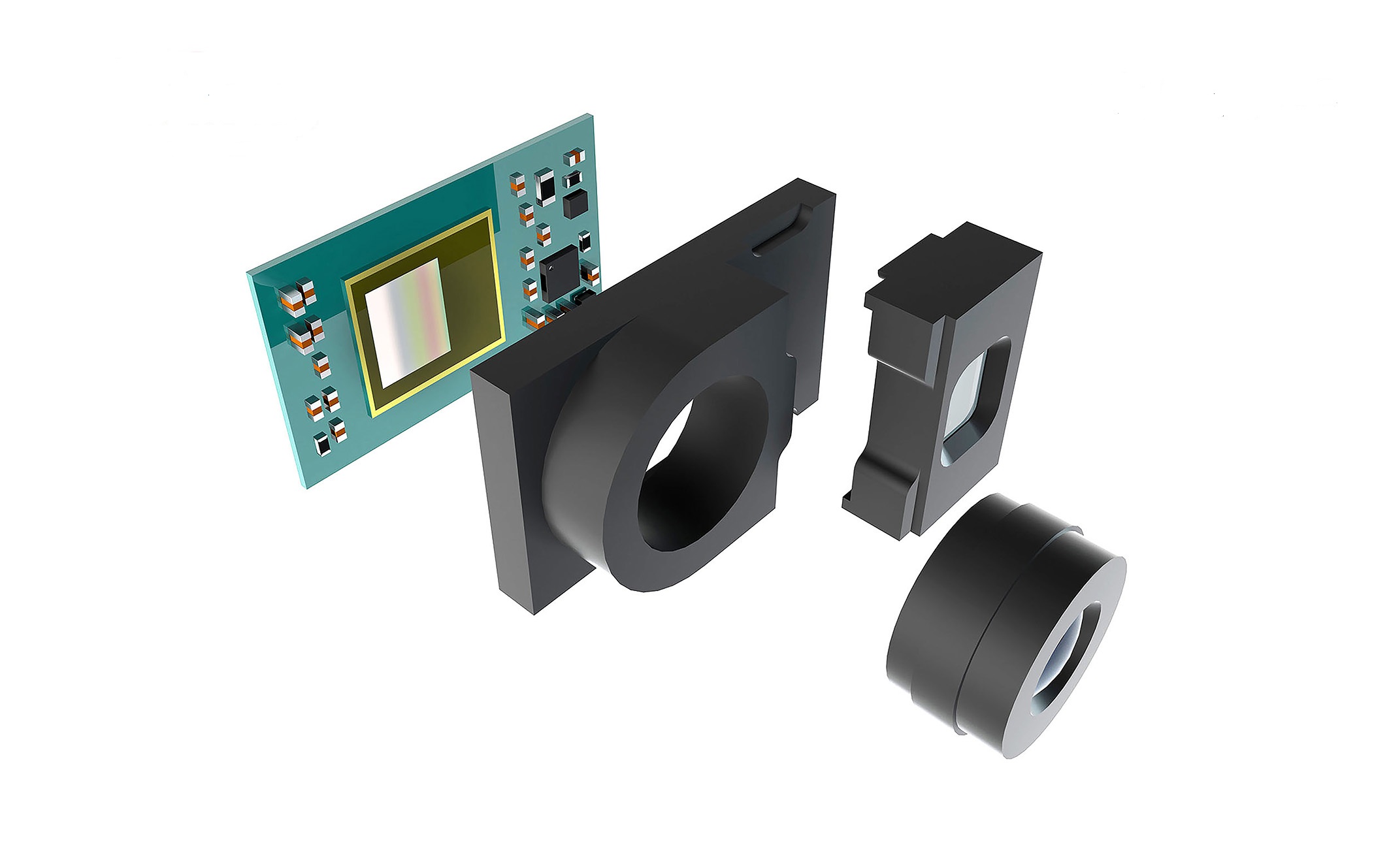
A 3D sensor comprises receiving optics and a VCSEL chip for object illumination. (Image: Infineon)
A 3D sensor is comprised of receiving optics responsible for the intensity of the emitted and reflected infrared light and a 3D-sensing chip of which the pixel sensitivity is crucial. The 3D-sensing chip, usually a VCSEL device, acts as a light source, illuminating the object like the human face with infrared light.
Take, for instance, facial recognition, wherein the VCSEL chip evenly illuminates the face with infrared light. Next, the 3D sensor captures key features of the user and compares them with the image of the user stored in the system. The smartphone will unlock if the two data sets match.
A VCSEL chip is much easier to install and, unlike laser diodes, is less sensitive to temperature fluctuations. That, in turn, paves the way for its use in automotive, industrial, and security applications.
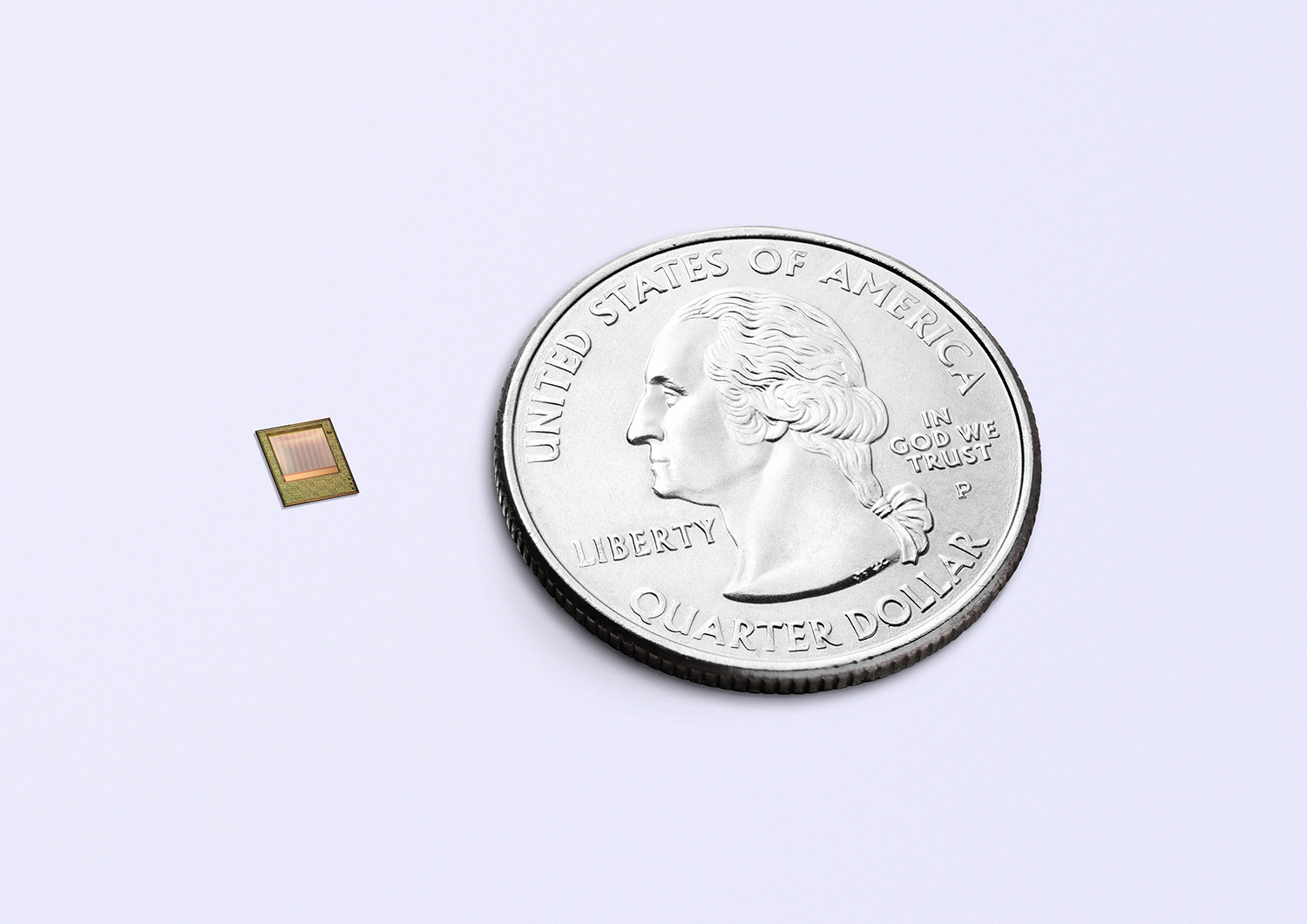
A 3D sensor based on a single-chip camera shrinks device size and reduces bill of materials. (Image: Infineon)
3D system integration
The optical sensing and imaging solutions mandate a complete and optimized hardware and software system. This also allows OEMs and system integrators to accelerate the deployment of 3D-sensing technologies in facial-recognition–enabled mobile payments, Animoji creation, and augmented and virtual reality.
That’s why 3D sensor supplier ams has joined hands with facial-recognition algorithm specialist Megvii’s Face++. The two companies are coordinating their design efforts to ensure that the 3D optical sensing hardware from ams and software algorithms of Face++ are optimized for each other.
The 3D optical sensing system from Austria-based ams employs infrared light projectors to map the surface of real-world objects such as a user’s face. Linking these 3D-sensing systems with facial-recognition algorithms enables designers to avoid the development risk and time associated with 3D-sensing software and hardware integration.
The Active Stereo Camera (ASC) reference design from Himax Technologies is another example of how integration works inside a 3D-sensing system. The 3D-sensing solution from Taiwan-based Himax is targeted at facial recognition and secure online payments for Android smartphones.
Himax has developed this 3D-sensing system in collaboration with mobile processor vendor MediaTek and Megvii, the Chinese developer of facial-recognition solutions built around the Face++ software. The ASC reference design combines MediaTek’s stereo matching depth engine and Megvii’s Face++-based computer-vision algorithm with Himax’s projector, sensor, and laser driver.
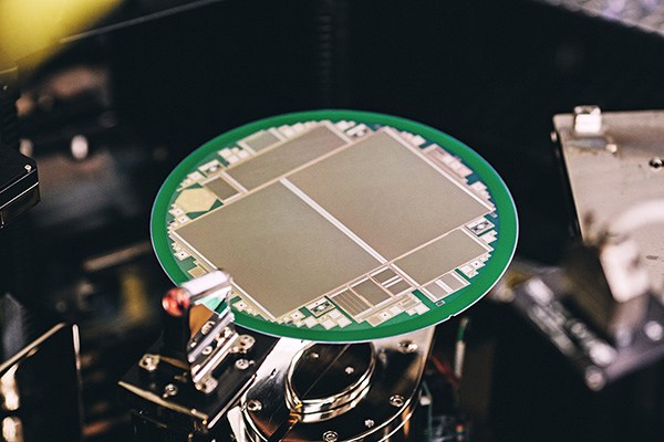
Infineon’s ToF-based REAL3 3D image sensor claims to enable a camera module with a footprint of less than 12 × 8 mm in smartphone designs. (Image: Infineon)
Himax has also teamed up with artificial intelligence (AI) specialist Kneron to take 3D sensors beyond smartphones to applications such as security and surveillance. Here, Himax is complementing its Structured Light Module (SLiM) with Kneron’s AI processor and facial-recognition algorithm to bring deep-learning technology to the network edge.
That allows the module to deliver 3D-depth map generation with greater resolution and accuracy for various applications. The 3D-sensing applications that SLiM facilitates in both indoor and outdoor environments include facial recognition, 3D reconstruction, and scene perception.
Next imaging revolution
The 3D-sensing designs have been propelled by initial entry into the smartphone world, but it took more than a decade to bring 3D optical sensing technologies such as facial recognition to smartphones. Now, a new wave of 3D-sensing applications is ready to power augmented reality, 3D mapping, robotics, drones, and more.
These optical sensing solutions — offering unprecedented levels of accuracy and image resolution — are optimized for a variety of scanning, facial recognition, and interactive systems. These 3D image sensors are also shrinking in form factor and power usage to enable use cases beyond facial recognition in smartphones.
For example, Occipital’s 3D sensor, Structure Core , offers 3D scanning and mapping on tablets and other mobile devices. Likewise, 3D-sensing systems are being employed in industrial applications such as materials processing and fiber-coupled laser pumping.
The 3D sensing and imaging revolution is here, and it will disrupt many markets. Look at how 3D sensing differentiated the iPhone X and how Android phones are struggling to equalize on this front. The IoT developers should take note because embedded systems could be a similar story.
Advertisement


