Battery fundamentals Part 4: Addressing common battery charging design challenges
Understanding the basics of battery technologies, charging, standards, charging IC features, and design traps minimize design challenges and reduce engineering time, cost and risk
BY GEORGE PAPARRIZOS
Summit Microelectronics
www.summitmicro.com
Part 1 can be found at: www2.electronicproducts.com/Fundamentals_of_battery_charging_Part_1-article-fapo_Summit_may2011-html.aspx Part 2 can be found at: www2.electronicproducts.com/Battery_charging_architectures_Part_2-article-fapo_Summit_jul2011-html.aspx Part 3 can be found at: www2.electronicproducts.com/Battery_fundamentals_Part_3_The_critical_charging_functions_and_parameters-article-fapo_Summit_P3_jul2011-html.aspx
With the majority of the portable devices having moved to Universal Serial Bus (USB) connectors as their standard connectivity and charging interface to the outside world, challenges associated with compliancy with the various USB and other standards have arisen. One significant side-effect of this market trend is the availability of power sources that may physically use the standard USB connectors, but may behave electrically very differently. Identifying such power sources allows the portable device to account for the corresponding power delivery, to meet certain industry specifications (such as USB battery charging) and to protect the downstream system from undesired voltage or current levels. Modern battery charging solutions exist that enable automatic power source detection and take corresponding actions based on their findings. Furthermore, such ICs recognize input sources even when battery voltage is low and system is off, thereby allowing for safe and fast charging independent of system condition.
Another obvious trend in portable electronics is the integration of higher levels of functionality, which in turn requires the use of larger displays, bigger batteries and new system-on-the chip (SOC) solutions, all of which are very power hungry. In such designs there are cases in which a power source may be attached to the portable device, however the system cannot power up immediately and may take a long time to wake up. Such a situation creates a negative customer impression, since the user cannot retrieve information from the portable device, or even worse, the user may think that the portable device is defective.
This scenario is very common when a portable system with a low battery (i.e. a battery voltage that is below or close to the system cut-off voltage level) is connected to a USB laptop port (also called standard downstream port) for charging. In this case, the 100 mA of current that is available for the device (USB specification) may not be adequate to wake up a modern system that requires significantly higher current for powering up, given that the deeply-discharged battery is not able to supplement any power. Until recently, only two solutions were possible to address this issue: 1) trickle-charging the battery for a long period of time, until it allows the system to power up, or 2) violating USB2.0 electrical specifications and allowing more than 100 mA (in most cases more than 250 mA!) to power up the system. A new technology, called Low-Battery Recovery (or LBR), is available that allows the steering of battery power directly to the system for a short period of time. This additional reverse boost operation does not require any additional external components and allows the charging IC to function like a 4.17-V step-up regulator for the system. In our practical scenario, this operation would enable the system to momentarily wake up, enumerate and increase the current from the USB port to 500 mA. Figure 10 demonstrates the LBR operation.
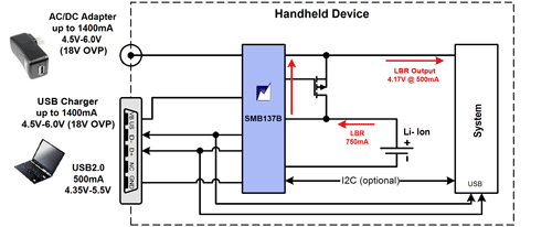
Fig. 10: Low-battery recovery mode for system power-up
Low-battery condition
When the battery is low or close to the point at which the system is allowed to wake up, there is also a risk of entering an oscillation mode, in which the system tries to wake up once certain conditions are met, but collapses again because it draws too much current out of the battery and thereby re-enters a low-battery condition. A possible solution to this common design issue is the use of charging solutions that can independently notify the system when to stay in standby mode and when to wake up. This is accomplished by the continuous monitoring of input power and battery voltage conditions and corresponding signaling between the charging IC and the system.
Board space limitation is another big challenge for most of the new portable applications. Ensuring a compact design requires keeping power dissipation to a minimum, since this reduces the need for a lot of copper or bigger case (i.e. larger industrial design) for being able to dissipate the heat. As previously discussed, switch-mode battery chargers provide high-efficiency power delivery to the system and battery. Many such modern solutions further contribute to space savings by utilizing modern package technologies that take no more space than the actual silicon! A very popular package type is the Wafer Level Chip-scale Package (or WLCSP), which allows a high number of Input/Outputs (I/Os) with the minimum possible x, y and z dimensions. Figure 11 demonstrates a solution that allows 15 I/Os while occupying only 2.1 x 1.3 x 0.6 mm.
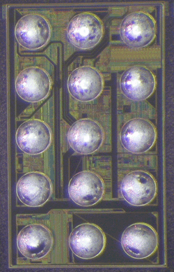
Fig. 11: Wafer-level chip-scale packages for space-saving battery charging solutions
Naturally, the space that the IC occupies is only a part of the design solution, since external components always need to be accounted for as well. Many of the latest switch-mode battery chargers operate at higher frequency levels, thereby allowing small chip capacitors and inductors and leading to overall board space reduction. In these cases, it is critical to ensure that switching frequency operation be constant over a wide range of operating conditions (input voltage, battery voltage, charge current), since varying frequency levels may introduce EMI challenges for applications utilizing wireless connectivity technologies.
As discussed in earlier sections, the high number of available USB wall adapters and corresponding cables on the marketplace may vary significantly in quality, current rating and electrical performance. As such, some of them output a voltage as low as 4.75 V (5 V ±5%) at their connector. However, additional voltage drops across the cable, the portable device connector and the PCB itself will further reduce this voltage level. This becomes a big challenge, especially with increasing current requirements (VDROP = ICHG x RDROP), since it may result in situations in which the input-to-output headroom of the battery charger is compromised, leading to slower charging rates (longer taper charging). While third party wall adapters, USB cables and consumer behavior cannot be well controlled, a careful layout that minimizes impedance across the power path and charging ICs with small FET resistances can mitigate some of the design risks.
The increasing popularity of electronic gadgets has driven a new wave of industry initiatives that target consumer satisfaction, product reliability and reduced electronic waste. Meeting all these new standards introduces new challenges in terms of design complexity, interoperability, system cost and size. Understanding the basics of battery technologies, battery charging, connectivity standards, new charging IC features and possible design traps can minimize design challenges and reduce engineering time, cost and risk. ■
Advertisement
Learn more about Summit Microelectronics


