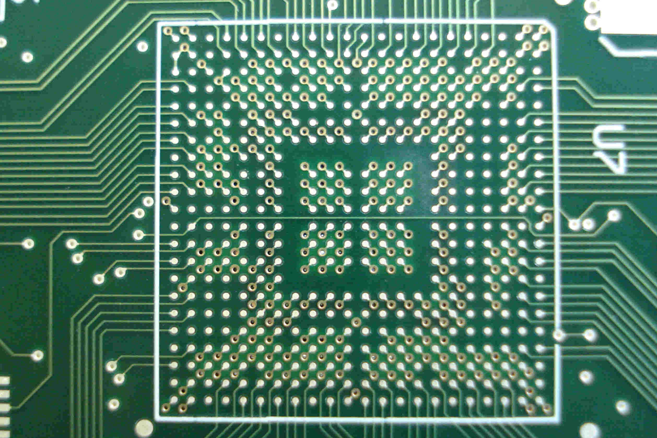
Ball grid array (BGAs) devices are, without question, an increasingly important aspect of printed circuit board design. While their benefits are numerous, they present the unique challenge of requiring an enormous amount of traces to originate in a small area underneath a device and then go all over the board without crossing traces. The most challenging aspect is getting those traces out from underneath the board, a process called creating a breakout or fanout. In the breakout, these traces are said to escape from underneath the board and come to the outside where they are more accessible. A poorly designed breakout can be overcome by increasing the layer count on a PCB but that increases the cost and complexity. There are number of different scenarios that would require different approaches to breaking out the races, however, due to limitations in space, only the more common concepts and methods will be discussed here.
When approaching a BGA breakout, there are several key features to watch out for. Foremost is the pin count, or how many balls there are on the device. Equally important is the pitch between the different pins. As the pitch decreases, the space available to run traces.
starts disappearing and the approach both in the fanout and the types of vias changes. There are different patterns used as well that will affect how you break it out, whether the balls are in perfect grids, in an offset pattern, if the pattern is different for different portions of the component, and if there are no pins in the center of the component. Finally, not dependent on the component, is the constraints given to you by your manufacturer. If you need more demanding constraints, you may need to look at a different manufacturer but that will cost more and there is a limit where even the most advanced manufacturers simply cannot go smaller.
Read full article
Advertisement
Learn more about Electronic Products Magazine


