By Brian Santo, contributing writer
Researchers at Brigham Young University have made an enormous leap in the production process for microfluidic devices. If the new 3D-printing process works as warranted, then science that relies on labs-on-chips should become significantly easier, cheaper, and faster.
Microfluidic devices enable large numbers of exceedingly small samples of fluids (measured in nanoliters and even picoliters) to be processed in parallel. Microfluidic devices, by definition, must have features with sub-millimeter measurements, but many prefer a stricter definition in which microfluidic device features should be smaller than 100 microns.
This isn’t just a semantic argument. The physics of fluids change at smaller regimes, and some of the new properties can be salubrious for some types of experiments. For example, flow ceases to be turbulent and becomes laminar. If there’s any interaction between two fluids, it has to be through diffusion, which can be useful to know when examining the interactions between the two.
Devices with features 100 nm and smaller have been made but not particularly inexpensively and not with 3D printing. Previous efforts with 3D printing “have not been in the truly microfluidic regime,” according to the BYU team, which subscribes to the
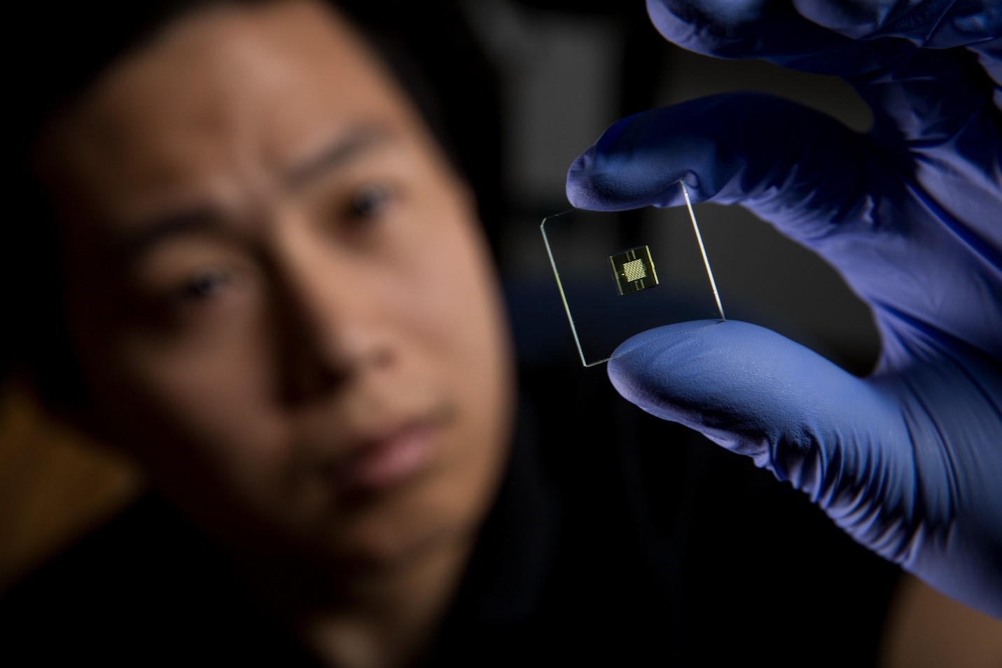
What BYU has just announced is a relatively simple 3D printing technique for mass-producing microfluidic channels with channels as small as 20 microns. The project was led by Greg Nordin, an electrical engineering professor at the university, and Adam Woolley, a chemistry professor.
EDA readers are likely to be more familiar with semiconductor production processes. Integrated circuits aren’t directly analogous to microfluidic devices, but they both rely on similar fabrication techniques. Imagine if the semiconductor industry had jumped from the 130-nm node straight to the 22-nm node without progressing through the 90-, 65-, 45-, and 32-nm nodes first. The improvement in microfluidics that the BYU 3D printing process promises is roughly as dramatic.
The researchers use a custom stereolithographic 3D printer (it uses digital light processing stereolithography, or DLP-SLA) which uses a 385-nm LED as a light source. In the past, DLP-SLA printers that have been used to fabricate 3D microfluidic devices have typically used a 405-nm LED. The BYU team said that going to a source with a shorter wavelength allowed them to experiment with a new set of resins; they say in their paper that they evaluated several and have settled on one that is low-cost and which can achieve flow channel cross sections as small as 18 x 20 nm.
The BYU researchers further said that they’ve succeeded in fabricating 3D serpentine flow channels 41 mm long in a volume of only 0.12 mm3 and by printing high-aspect-ratio flow channels
Every method available to date for making microfluidic devices has advantages and drawbacks. There are several etching processes used to make silicon and glass devices; these processes work just like the etching process in semiconductor production. Precision manufacturing is possible, but silicon and glass are expensive compared to the use of polymer resins. Furthermore, silicon and glass are not ideal for use in biological applications for several reasons.
The properties of polymer resins tend to make them better for biological applications, though polymers degrade faster than silicon or glass. One set of production techniques uses heat to prepare polymer materials for embossing or injection molding. Another set of approaches relies on micromachining or lasers to cut polymer materials into desired forms. There are also several casting techniques that use a mold (sometimes silicon) to stamp a polymer resin. Working with polymers usually entails lower cost and faster manufacturing speed, but the sacrifice is almost always in precision.
This is why the new 3D printing technique from BYU is considered exciting. It is precise in addition to being less expensive and fast. The approach can create a device in 30 minutes and does not require the use of clean rooms, the researchers told BYU News .
“It’s not just a little step; it’s a huge leap from one size regime to a previously inaccessible size regime for 3D printing,” said Woolley. “It opens up a lot of doors for making microfluidics more easily and inexpensively.”
Microfluidics have become common in several endeavors. They can be used in biology to process samples with various reagents, including DNA samples and new drugs. The existence of smaller devices will be a boon for any number of reasons. For starters, it will be easier to simply fit more samples in a smaller area.
Another example is based on the popularity of a particular nematode (c. elegans) as a test subject in biology. But there’s a need to immobilize the worms to observe them. Confining them to tiny channels does the trick.
Advertisement
Learn more about Electronic Products Magazine


