By Jennifer Cheney
Staff Applications Engineer
Keithley Instruments, a Tektronix Company
www.keithley.com
High-voltage capacitance-voltage (HV C-V) measurements are an increasingly important for characterizing the latest generation of wide-bandgap power semiconductor devices because the measurements are useful in predicting such key dynamic device characteristics as switching time and gate charge. But making HV C-V measurements on power semis is no trivial task. The high voltages demand extra precautions for personal safety, to deal with system capacitance issues, and to protect instruments from over-voltages.
HV C-V measurements require use of a carefully selected bias tee, a device that combines the high-voltage bias signals from an SMU instrument with ac measurement signals from the capacitance instrument, at the same time isolating the instruments from each other. The capacitor of the bias tee blocks the SMU instrument from interfering with the capacitance meter; and the inductor blocks the C-V meter from interfering with the SMU instrument. Since a power semi’s capacitances are a function of voltage, to obtain a complete picture of device switching behavior, designers need to measure capacitance up to the maximum voltage of the device.
Tees for C-V measurement
Typical RF-instrumentation bias tees have drawbacks for power semi testing. These tees are designed only for ac measurements, operate over a specific frequency range, and have a coaxial design. Characterizing power devices, however, demands making a number of other measurements, both on-state and off-state. Making off-state measurements, such as characterizing a device’s zero-gate-voltage drain current (IDSS ), are particularly difficult to perform through a coaxial bias tee, because they often require measuring current at microamp or nanoamp levels. Traditional coaxial bias tees have high leakage, which often results in a noise floor that’s higher than the device measurement. In order to measure these low currents, test engineers have typically been forced to perform dc I-V measurements first, then have to re-cable and re-configure the system for C-V measurements. Obviously, this approach is less than optimal: constant recabling/reconfiguration is both time-consuming and prone to errors.
A better solution is a multi-mode triaxial bias tee that can remain in place for both C-V and dc I-V measurements (fig. 1 ). The triaxial design ensures more accurate low-current dc measurements because the SMU guard is the triax inner shield and the ac Return/Ground is the triax outer shield. The triaxial bias tee minimizes the need for connection changes at the probe side of the device interface. In addition to low leakage, this design offers switches that let users configure to optimize the path for the desired type of measurement. With the appropriate software, theses switches can be configured automatically for the measurement desired. The connections between the output of the bias tee and the DUT are the same for both I-V and C-V measurements.
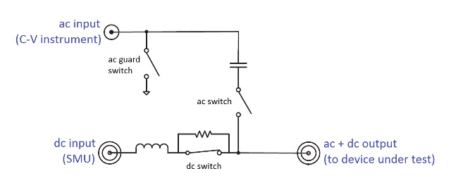
Fig. 1: Multi-mode triaxial bias tee design
Capacitance capacity
Measuring the capacitance between two device terminals on 3- and 4-terminal devices is another significant challenge, because parallel capacitance paths and large ratios between device capacitances have a significant impact on measurement accuracy and resolution.
Those evaluating MOSFETS in switching power supplies are often interested in the circuit-level capacitances—the input, output, and transfer capacitances—which are combinations of the terminal-level capacitances (fig. 2 ). Capacitance measurements on power devices like MOSFETs are challenging because the capacitance to be measured is interconnected with other device capacitances. The ratio between capacitors also affects measurement accuracy, as illustrated by the challenges associated with measuring a power MOSFET’s input capacitance (CISS ) (fig. 3 ).
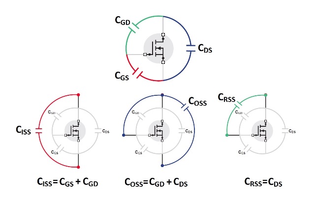
Fig. 2: Terminal-level capacitances.
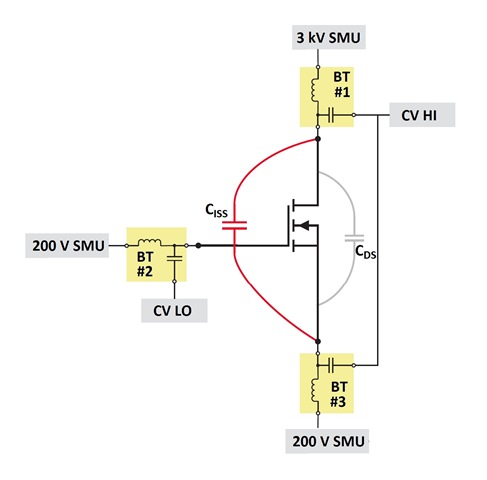
Fig. 3: Measuring a power MOSFET’s input capacitance. Note that the capacitance of BT #3 shorts out CDS if the capacitance of BT #3 is significantly greater than CDS .
Measuring CISS with multi-mode bias tees means using a bias tee on each terminal of the device and an SMU instrument at each terminal. This permits applying a dc bias at each terminal.
When measuring CISS , the biggest challenge is that the capacitance between the drain and source terminals affects the accuracy of your measurement. Fig. 4 shows how the capacitance of the bias tee at the source terminal (BT #3) helps reduce this issue. The capacitance of the power MOSFET is represented in fig. 4 in a simple 3-terminal model.
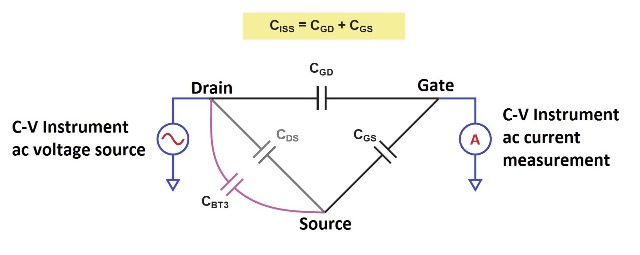
Fig. 4. A 3-terminal model of the capacitance of a power MOSFET. Since CBT3 is significantly greater than CDS , the ac drain and source voltages are approximately the same and the measured capacitance is equal to CISS .
Whatever ac current is generated by the C-V meter flows through all three terminal-level capacitances. A capacitor is needed to “short out” CDS so that the same ac voltage that appears at the drain also appears at the source terminal of the FET. This shorting capacitor must be much larger than CDS , so that it is a much lower impedance. It must also be rated for high voltage, because high voltage is present at the drain terminal during a C-V measurement of a power MOSFET.
With this shorting capacitor in place, no ac current flows through CDS , so the ac current measured by the C-V meter is just that due to CGD and CGS , the components of CISS . The capacitance of the bias tee at the FET’s source terminal is an effective solution for this shorting capacitor. It can be connected using cables at the low voltage input side of the bias tee. These multi-mode bias tees also greatly simplify measurements of the remaining circuit level (COSS , CRSS ) and terminal-level (CGS , CGD , CDS ) capacitances. Too, by allowing a bias at every terminal of the device, it becomes easy to measure capacitances of depletion mode devices, such as GaN transistors, without additional hardware. These triaxial multi-mode bias tees can allow making high voltage C-V measurements on commercially available 3,000-V power devices.
Conclusion
Validating power semiconductor devices demands careful attention to selecting the right instrumentation, connectors, and cabling. For more information on the selection process and the options available, I’d encourage you to watch my online webcast, Learn How to Validate Power Semiconductor Device Designs Simply and Accurately, available at http://info.tek.com/power-semi-webinar.html.
Biographical Note
Jennifer Cheney is a Staff Applications Engineer at Keithley Instruments, Inc., headquartered in Cleveland, Ohio, which is part of the Tektronix test and measurement portfolio. She earned a Bachelor of Science degree in electrical engineering from Case Western Reserve University in Cleveland. She has been assisting Keithley customers with instrument applications since 2001.
Advertisement
Learn more about Keithley Instruments


