BY TED MARENA
Director of Solutions Marketing
Lattice Semiconductor
www.latticesemi.com/csi2bridge
The majority of cameras in high volume consumer products, such as smartphones and tablets, use MIPI (Mobile Industry Processor Interface)-based sensors. The most commonly used interface for this type of image sensor is the CSI-2 specification (Camera Serial Interface). CSI-2 consists of a unique physical bus that contains a differential clock and from one to four differential data lanes. This interface is called a D-PHY. What makes the D-PHY unique is that it can change “on the fly” from differential to single-ended signaling. High Speed (HS) mode is differential and single-ended mode is called low power (LP). For an high performance video from a CSI-2 image sensor will use the HS differential data mode.
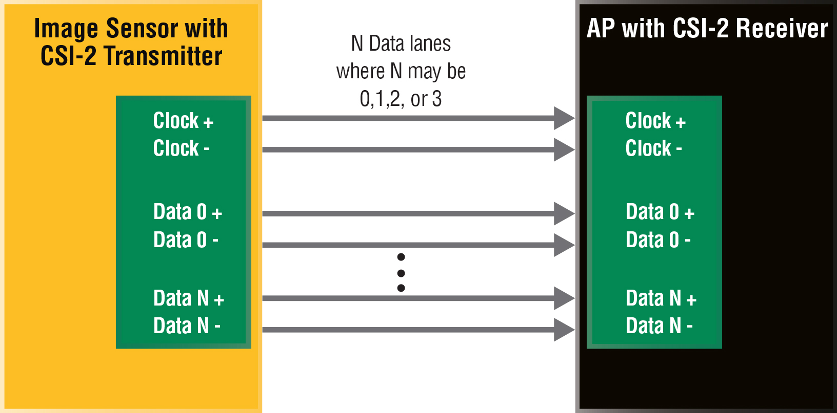
The CSI-2 HS interface operates electrically as a SLVS (scalable-low-voltage-signaling) standard device with a 200 mV common mode voltage. The clock is DDR source synchronous and the number of data lanes for a CSI-2 interface can vary from one to four lanes. Each data lane transmits 8-bit serial data. The higher the image sensor resolution and frame rate the more data lanes, and higher speed for each, will be required. The practical limit for a CSI-2 interface is less than 1 Gbits/s data rates, but often it is less than 700 Mbits/s. For example, a high definition 1080p60 video signal would be transmitted with four differential data lanes, each running up to about 500 Mbits/s. Figure 1 shows a typical block diagram.

Figure 1: A CSI-2 sensor interface
In many of these applications the CSI-2 image sensor would be configured at power up and set to transmit the frames in HS mode continuously. This is free running clock mode or fixed high-speed mode.
The challenge for these non-consumer-based camera designs is that most do not use an applications processor, instead they may have an image signal processor (ISP) or a microcontroller without a CSI-2 interface. They may use a traditional CMOS bus for their camera interface. MCUs with a parallel CMOS interface bus cannot be connected directly to a CSI-2 image sensor like an AP can. For these designs an external bridge is needed (see Fig. 2 ).

Figure 2. CSI-2 to CMOS Parallel Block Diagram
A low density FPGA is an ideal component for this bridge design, and reference designs are available for this method. For example, the Lattice MachXO2 FPGA has a bank of configurable differential I/Os that can be leveraged to support the CSI-2 HS interface. If the end application can use the CSI-2 image sensor in free running clock mode, then the implementation is straightforward with a seamless connection between the devices. If both HS and LP modes need to be supported, then the MachXO2 FPGA can support this with external discrete components and additional I/O pins. From one to four data lanes are supported with data rates of up to 750 Mbps.
The 1200 LUT density of the this FPGA can create a two lane CSI-2 to parallel bridge to support the free running clock mode. To support 1080p30 resolution, the device would consume 66 mW and require no external components. If the image sensor is used in both LP and HS mode, then the power consumption when in LP mode would be 30 mW. Overall, the FPGA density size and power will be dependent on the number of CSI-2 data lanes, the resolution and how many modes are needed. This FPGA solution allows a user to configure a CSI-2 interface for their specific requirements.
Advertisement
Learn more about Lattice Semiconductor


