Cell-based ASICs dominate new offerings as processes dip below 0.2 µm
Proprietary libraries are augmented
by cores licensed from third-party intellectual-property firms
BY RODNEY MYRVAAGNES
Associate Editor
The leading-edge ASIC houses are bringing up processes this year with drawn features smaller than 0.2 µm, continuing the push to system-on-chip functionality evident in the last two generations. Gate arrays manifest themselves mainly in conversions from programmable logic and from twilight production lines. These show up in older process technologies of 0.35 µm and larger.
Each new process generation shrinks the largest device previously possible so that the device takes up only a fraction of a new chip with the same area. The G10, G11, and G12 generations from LSI Logic (Milpitas, CA) illustrate this progression (see Fig. 1 ).
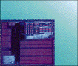
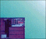
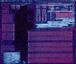
Fig. 1. The last three generations of system-on-chip offerings from
LSI Logic dramatize the space gained with each new process.
This is a blessing for industries with insatiable demand for the same silicon repeated many times over, such as switchgear. If a big switch contains 1,000 identical microprocessors, just getting more of them on each chip reduces costs or lets more lines be handled with the same size circuit board. But other industries can only make use of the technology by bringing many different board-level functions on chip. They can only do this when the end product has a large enough market to justify the NRE costs.
Advanced processes
IBM Microelectronics (Essex Junction, VT) has current bragging rights for its six-metal-layer process with copper interconnects available (see Fig. 2 ). The drawn features of the SA-27 process are 0.16 µm in size.
Fig. 2. IBM's newest process, the copper-connected SA-27,
offers up to six metal layers with 0.16-µm drawn gate lengths.
The contacted pitch in the third and higher metal layers is 1.26 µm. Local interconnects are 0.84 µm. Gate delays are down to 33 ps. Several other companies are working to make copper interconnects practical, but are not quite there yet.
However, LSI Logic's G12 process offers much else. The cell-based family has drawn features of 0.18 µm and three, four, five, or six layers of metal interconnect as they are needed. A low-k dielectric is used in the metal layers, allowing a 0.63-µm fully connected metal pitch. Usable gate capacities extend to 26 million on a 20 x 20-mm chip, with 0.5 million to 8 million typically used (see Fig. 1 ).
The G12 devices operate at 1.0 or 1.8 V internally, with a wide assortment of 3.3-V I/O options. In addition, the chips can include such mixed-signal functions as data conversion, data transport, and signal processing.
At 1.0 V, the devices dissipate about 7 nW/gate/MHz. Both transistors can be present on the same chip. Prototype designs will begin in the fourth quarter, with initial production ramping up in the second quarter of 1999. (Also see Outlook, page 24.)
Gate arrays
Gate arrays will, no doubt, continue to be produced well into the future. However, new gate-array offerings have dwindled. Conversions of programmable-logic designs are on the upswing.
American Microsystems (Pocatello, ID) has been active in the conversion business for years, and claims over 1,000 successful netlist conversions, both from FPGA designs and gate-array formats of other vendors. The company offers to convert any FPGA in existence.
The company is actively wooing customers from older Motorola Semiconductor and VLSI Technology fabrication lines for its 8-in. submicron facility, which will be producing designs down to 0.35 µm by the end of the year.
A more specialized conversion service, Integrated Logic Systems (Colorado Springs, CO) offers metal-programmed gate arrays specifically
designed to replace FPGAs and CPLDs from Actel, Altera, and Xi-linx. The MPGA III family is fabricated in 0.5-µm CMOS with three metal layers. The topmost layer is customized, and the conversion is simple enough to eliminate NRE charges on orders of 4,000 or more parts. Capacities range to 31,000 gates and 28,000 bits of dual-port RAM.
Chip Express (Santa Clara, CA) has added the CX3000 family (see Fig. 3 ) to its line of laser-programmable gate arrays (LPGAs).
Fig. 3. The Chip Express laser-burned gate array
can be programmed overnight for prototypes.
Like the company's previous lines, the laser-burned devices are backed by architecturally identical gate arrays for production. After a laser-burned CX3001 prototype is accepted, small production runs of identical “one-mask” devices can be made on premises. Finally, for high-volume production, the CX3002 follow-on devices are produced at the foundry.
Embedded DRAM
Because of the process difference between commodity DRAMs and logic chips of any sort, the two make uncomfortable chipfellows. However, the prospect of cutting off-chip traffic becomes a more compelling argument for DRAM-logic integration with each generation.
Companies with this capability include Mitsubishi Electronics America (Mountain View, CA), whose pioneering MR32R/D microprocessor is advancing to new generations.
Toshiba America Electronic Components (San Jose, CA) has its own process, which it has licensed to Chartered Semiconductor (Taiwan), a foundry for many fabless semiconductor companies.
Intellectual property
Licensed intellectual property in the form of cell designs has become a major component of the cell libraries of all major ASIC vendors. Two items in particular, the ARM7-TDMI microprocessor and the OakDSPCore digital signal processor, are almost universally available, and their success has spawned an industry.
VLSI Technology (San Jose, CA), a long-time ARM licensee, offers its own enhancements to the ARM and Oak cores in its Multicore family of telecommunications devices (see Fig. 4 ). It has also begun offering the new ARM9TD, which is expected to be capable of 180 native MIPS by the fourth quarter.
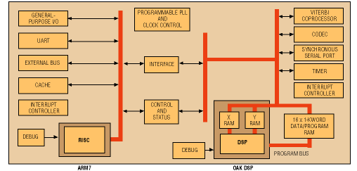
Fig. 4. VLSI Technology's Multicore family combines third-party
ARM and Oak processors with the company's in-house library to create telecom parts.
The ARM9TD features a five-stage pipeline, a Harvard bus architecture, embedded debugging, and back compatibility with both 32- and 16-bit ARM instruction sets. The company's Oak+ (VLSI Technology's name for the enhanced core) operates at 130 MIPS in a 0.25-µm process. It offers access to both x and y data buses off core, permitting designers to balance traffic between the two.
NEC Electronics (Santa Clara, CA) will add its own 1394 OPCI-Link to its ASIC libraries in the second half of the year. The device supports the IEEE 1394 Open Host Controller Interface, a standard that will allow consumer and computing devices to communicate on the same physical medium. The company has also licensed 10/100-Mbit/s and Gigabit Ethernet MAC cells from Packet Engines, along with other Ethernet-related cells.
Samsung Semiconductor (San Jose, CA) has recently opened worldwide ASIC design services, with core libraries aimed at communications, portable computing, and consumer system-on-chip products. The company's ASIC process is based on that of the 600-MHz 21164 Alpha. It incorporates added mixed-signal capabilities not used in the Alpha.
New embedded SRAM and flash capability is an extension of the company's merged DRAM and logic efforts. The flash entails six added process steps on the standard CMOS. The embedded SRAM ranges from 1 to 4 Mbits, with 256-bit buses and 100-MHz clock rates possible, for a peak bandwidth of 800 Mbytes/s.
Siemens Microelectronics (Cupertino, CA) offers its in-house TriCore-1 as a cell. The 32-bit processor combines control and DSP tasks in one instruction set. Siemens can combine the TriCore-1 with as much as 2 Mbytes of DRAM, or 1 Mbyte of flash memory.
The company's library includes a wide range of microcontroller peripheral blocks. The TriCore-1 itself includes a proprietary flexible peripheral interconnect bus that supports data rates up to 800 Mbytes/s.
Mitel Semiconductor (San Jose, CA), formerly GEC Plessey Semiconductors, offers both cell and gate-array ASICs in a 0.35-µm CMOS process. The GSC200 cell-based family is optimized for low-power applications. At 2 V, a two-input NAND with two loads draws 0.07 µW/MHz.
Core and I/O cells can be operated independently at 2 or 3 V, and 5-V tolerant I/O cells are available. The library includes oscillators and PLLs, as well as the ubiquitous ARM7-TDMI and the OakDSPCore (see Fig. 5 ).
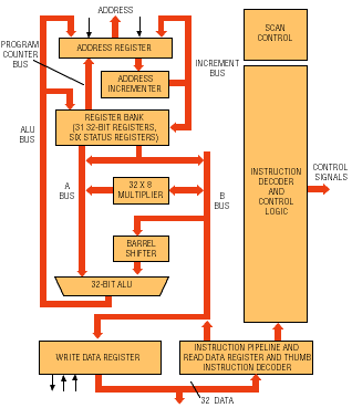
Fig. 5. The ARM7TDMI microprocessor shows up as a library core cell
in many vendors' offerings.
Lucent Technologies (Allentown, PA), a minority owner of Chip Express, will jointly develop a 0.25-µm version of that company's LPGA to be incorporated as a cell in Lucent's system-level ASICs, thus leaving a portion of its ASICs uncommitted. These chips will be offered with the same laser and one-mask services that Chip Express offers. No date for production has been announced.
The following companies contributed information for this article:
Advertisement


