Characterization system checks power devices at wafer level
System allows testing of die at 60 A, 3,000 V without the need for preprocessing or ad-hoc test setups
The Tesla power device characterization system lets engineers perform overtemperature low-contact-resistance measurements of power semiconductor die at the wafer level for the first time. Previously, engineers had to have devices packaged prior to characterization and model extraction, resulting in extra cost and delays, because ad-hoc wafer-level measurements resulted in unreliable or inaccurate data.
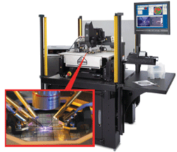
The system features two new wafer probes, one for a high current and another for high voltage. The high-current probe, which can support up to 10 A of continuous current mode and 60 A of pulsed current, reduces device heating by minimizing contact resistance at the wafer-to-probe interface, while the high-voltage probe can make coaxial measurements up to 3,000 V and triaxial ones to 1,100 V. Both probes’ tips are easily replaced.
The system’s wafer chuck can handle thin wafers using an exclusive technology. The technique provides just the right amount of vacuum in a delicate method that protects against wafer breakage and probe damage, all while ensuring a minimal contact resistance. Other safety features include high-insulation shielded cable assemblies for triaxial performance and high-current/high-voltage handling, a safety interlock system, and remote system operation. (From $200,000available 12 weeks ARO.)
Cascade Microtech , Beaverton , OR
Information 503-601-1000
Advertisement
Learn more about Cascade Microtech


