A processor chip developed by researchers at MIT might soon make it possible to change the overly-flawed smartphone snapshot into a professional looking photograph with no more effort needed than the simple push of a button.

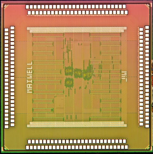
Die photo of MIT’s new processor chip.
The chip was developed by a team at MIT’s Microsystems Technology Laboratory. Capabilities include creating more realistic imagery as well as enhancement of the lighting in a shot without destroying the scene’s ambience.
Also worth noting is the fact that the chip is universal in that it can be incorporated into any smartphone, tablet, or digital camera presently on the market.
Major improvement in smartphone camera technology
The problem with today’s smartphone cameras can be found in the photography system’s software application; specifically, the amount of power it consumes, time it takes to run, and the amount of know-how it takes for the user to be able to use it effectively. This is all according to Rahul Rithe, a graduate student in MIT’s Department of Electrical Engineering and Computer Science who worked on this project and is the lead author on the paper the team turned out after working on this project.
“We wanted to build a single chip that could perform multiple operations, consume significantly less power compared to doing the same job in software, and do it all in real time,” Rithe says.
High Dynamic Range Imaging
One thing that the chip can do is a task called High Dynamic Range (HDR) imaging. It’s designed to make up for the limitations of brightness able to be recorded by today’s digital cameras. In doing this, it is able to capture snapshots that more accurately reflect the way in which we observe the same scenes with our eyes.
In order to do this, the chip’s processor automatically takes three separate “low dynamic range” images with the camera:
• Overexposed image to capture the details of the dark areas in the scene
• Underexposed image to capture details in the bright areas of the scene
• Normally exposed image
It then merges these three images together to create one image that captures the entire range of brightness. And it’s all done in the blink of an eye. Where most of today’s software-based systems take several seconds to perform a similar operation, the MIT chip can perform this task for a 10-megapixel image in just a few hundred milliseconds. What’s more, it can be applied to video too, and all with less power than existing CPUs and GPUs.
Additional advantages
Along with improving the lighting in digital photographs, the chip can enhance the lighting in a darkened scene better than conventional flash photography. “Typically when taking pictures in a low-light situation, if we don’t use flash on the camera we get images that are pretty dark and noisy, and if we do use the flash we get bright images but with harsh lighting, and the ambience created by the natural lighting in the room is lost,” Rithe explains.
What the chip does instead is it captures two images at once—one with a flash and one without. It then splits both images to just the large-scale features within the shot, and a detailed layer. From there, it merges both images while at the same time preserving the natural ambience from the base layer of the non-flash shot and extracting the details from the picture taken with the flash.
To remove noise, the chip blurs any undesired pixel with its surrounding neighbors so as to match those around it. This might raise a flag to those familiar with photography as a feature like this typically means these pixels at the edges of objects are also blurred, thereby resulting in a damaged / less detailed image. Fortunately, this is not the case with the MIT chip. You see, the system uses a bilateral filter, which allows the user to preserve the outlines in their snapshot. It only blurs pixels with their neighbors if they’ve been assigned a similar brightness value. Since any objects within the image are likely to have a very different level of brightness than that of their background, this prevents the system from blurring across any edges, Rithe says.
It sounds simple enough when written to paper, but to actually do this, the CPU uses a bilateral grid to organize and store data: the image is divided into smaller blocks first, and for each block, a histogram is created. This results in a 3D representation of the image, complete with x and y axes representing the position of the block, and the brightness histogram representing the third dimension. By doing this, it’s easier for the filter to avoid blurring across edges since pixels with different brightness levels are separated in this third axis.
Outlook
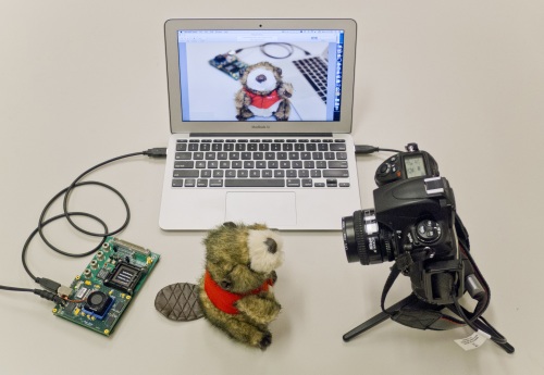
With help from Taiwanese semiconductor manufacturer TSMC’s University Shuttle Program, the MIT group has already built a working prototype of the chip using 40-nanometer CMOS technology, and integrated it into a camera / display model.

Group’s demonstration system integrates processor with DDR2 memory and connects with camera / display via USB interface.
They will present the technology at the Internal Solid-State Conference in San Francisco.
Thoughts on this new technology? Post them to the sensors forum on DigiKey’s TechXchange.
Story via: MIT.edu
Advertisement


