Closer molecular packing more than doubles organic semi’s conductivity
Researchers at Stanford University led by chemical engineer Zhenan Bao have created organic semiconductors with conductivity more than twice that previously achieved. The improvement could result in practical flexible electronics, as well as solar cells with higher efficiency and improved displays.
The improvement was achieved by growing organic semiconductor crystals with the molecules packed more closely together (see Fig. 1 ), a process the referred to as lattice straining. The result is an eleven-fold increase in performance compared the same semiconductor material with unstrained lattices.
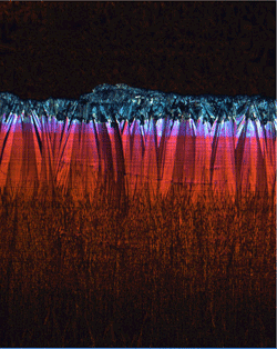
Fig. 1. Tightly packing the molecules in an organic semiconductor lattice as seen here more than doubles its electrical conductivity. (Photo credit Gaurav Giri / Stanford University)
While using strained lattices is not uncommon for silicon ICs, Bao points out that, “no one has been successful in creating a stable strained lattice organic semiconductor with a very short distance between molecules, until now.”
Previous attempts to grow organic semiconductors under high pressure did not prove stable; once the pressure was released, the lattice would return to its unstrained state.
To overcome the problem Bao and her team mates —Stanford doctoral candidates Guarav Giri and Eric Verploegen, former post-doctoral scholar Hector Becerril, and Stefan Mannsfeld and Michael F. Toney of the Stanford Synchrotron Radiation Lightsource — used a technique similar to a common silicon-semiconductor coating process: solution shearing. A thin, liquid layer of the semiconductor material was sandwiched between a heated lower metal plate and an upper metal plate that floats atop the liquid. When the top plate moves across the liquid, its trailing edge exposes the liquid to a vaporized solvent and a thin-film crystaline semiconductor is formed on the heated plate.
To understand the compressed lattices structures and their characteristics, measurement and visualization of the lattices was conducted by Stefan Mannsfeld, an X-ray scattering expert in at the Stanford Synchrotron Radiation Lightsource. In his words, the team was “able to improve how we analyze the relative brightness of the peaks we can see in X-ray diffraction images. Previously this was only possible when analyzing relatively big single crystals….” Imaging made it possible to see the impact of the strain on the lattice geometry and determine the exact way in which the molecules are packed.
To control semiconductor properties during solution shearing, engineers can vary the speed at which the top plate moves, the thickness of the solution layer, and the temperature of the lower plate. For the material used by the researchers, engineers found that optimal electrical conductivity was achieved when the top plate moved at 2.8 mm/s. Bao notes that, “Using a process so similar to current industry technology is important, as it could speed these new semiconductors to market.” For further information, contact Zhenan Bao at 650-723-2419 or zbao@stanford.edu
Richard Comerford
Advertisement
Learn more about Stanford University


