CIRCUIT FUNCTION AND BENEFITS
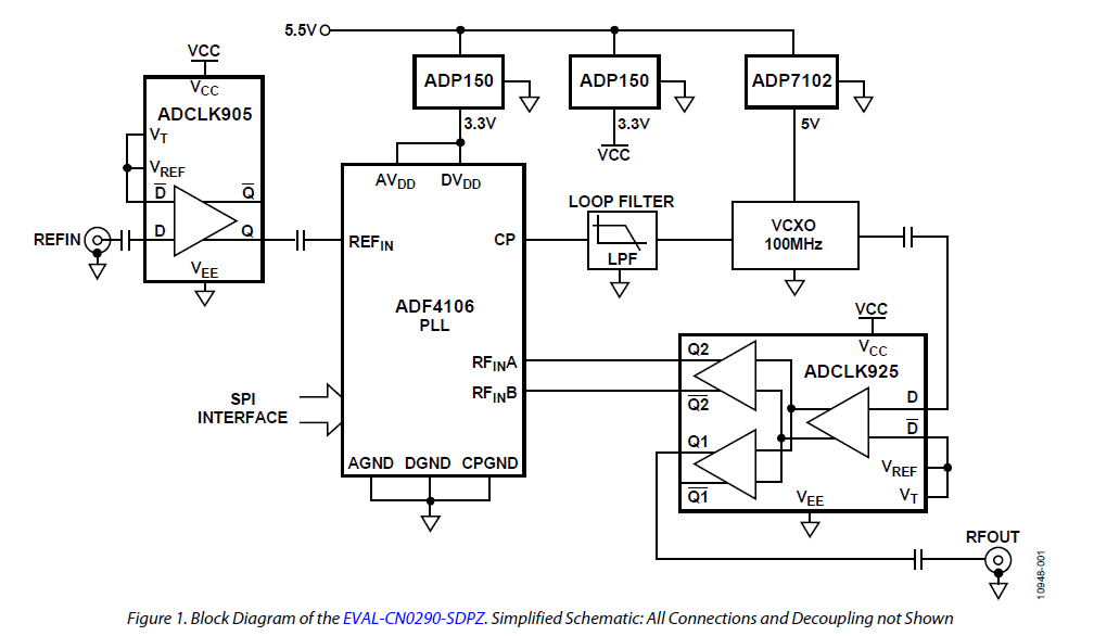
The circuit shown in Figure 1 is a high performance phase locked loop (PLL) that uses high speed clock buffers and low noise LDOs to maintain low phase noise even at low reference and RF frequencies.
For example, the minimum reference frequency and the RF input frequency of a number of Analog Devices PLLs, such as the ADF4106, are specified for 20 MHz and 500 MHz,respectively. The frequency range can be lowered to a 10 MHz reference frequency and a 100 MHz RF input using the additional clock buffers as in Figure 1.
Download Full Block Diagram Below
Advertisement

Learn more about Analog Devices


