Combining simulation & measurement in design
Going forward, integrated design and test practices will be major factors in improving engineering design excellence
BY DAVID HALL
Senior RF Product Manager
National Instruments
www.ni.com
Shortening the product development cycle has long been a key objective of R&D organizations. One method to reduce development time is concurrent design and test — often practiced in the form of the V-diagram product development model. This has been used especially in the automotive and aerospace industries.
In these industries, where the end product is a highly complex “system of systems,” the left side of the V diagram is considered design, and the right side represents test/validation (see Fig. 1 ). The idea behind the V diagram is that greater efficiency can be achieved by beginning the test and validation of subsystems before development of the entire system is complete.
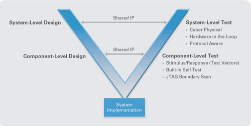
Fig. 1: When designing large systems of systems, the V diagram is a convenient way to visualize which subsystems can be tested independently of the entire system.
While the use of concurrent design and test approaches such as the V diagram is common in industries with highly regulated environments, adoption of these practices is growing in other industries and for other types of devices as well. For example, in the semiconductor and consumer electronics industries, shorter product lifespans and increasing product complexity continually drive pressure to reduce product development time.
According to a 2009 McKinsey survey on fabless semiconductor design processes ( www.mckinsey.com/Client_Service/Semiconductors/Latest_thinking/Getting_More_out_of_semiconductor_RD), the ratio of product lifecycle to product development type in the semiconductor industry is approximately one third of what it is in the automotive industry. The same McKinsey survey estimates that the average development time of a new semiconductor design is approximately 19 months. For this reason, they claim that R&D excellence is a key differentiating factor.
Given the business imperative for improving R&D excellence in the product development process, the goal of concurrent design and test has become widespread throughout the electronics industry. A key method to empower this practice is increasing the connectivity between electronic design automation (EDA) simulation software and test software all the way to the component level.
In-process software use
To understand the role of simulation software in the product design flow, it’s important to understand the role of software in both the design and test phases of product development. During initial design and simulation, EDA software is used to model either the physical or electrical behaviors of a simulated product. Effectively, we can think of the EDA software as a utility that uses mathematical models to represent the output of a device under test (DUT) based on a series of inputs — and then presents these metrics to the designer.
During the validation/verification stage of product development, engineers use software in a slightly different context — namely to automate measurements on a real prototype. However, similar to the design and simulation phase, the V&V process requires measurement algorithms as those used by EDA software tools.

Fig. 2: Software plays a key role throughout the development cycle.
One emerging feature in today’s EDA software is the ability to provide increasing levels of software connectivity between the EDA environment and test software. More specifically, this connectivity enables (1) modern EDA software environments to drive measurement software, and (2) measurement automation environments to automate the EDA design environment.
One benefit of connectivity between design and test software environments is that it allows design engineers utilize significantly richer measurement algorithms earlier in the design process. Not only do engineers gain more valuable knowledge of their design earlier in the design process — but it also affords the opportunity to correlate simulations with measured data from the V&V process. A second benefit of increased connectivity between EDA and test environments is that it allows test engineers to develop working test code much sooner in the design process — ultimately reducing time to market for complex products.
EDA enriching measurement
One way that EDA and test software connectivity improves the design process is through richer measurements. Fundamentally, EDA tools use behavioral models to predict the behavior of a new design. Unfortunately, the modeled design is often verified using measurement criteria that are ultimately different than what will be used to verify the final product — making it difficult to correlate simulated and measured data.
One growing trend is to use a common tool chain for design through test — a trend that ultimately enables engineers to introduce measurements earlier into the design flow.
For example, consider the design of a cellular multimode RF power amplifier. Traditionally, this type of part is designed and modeled using RF EDA tools such as AWR Microwave Office. Using the EDA environment, engineers typically “measure” RF characteristics such as efficiency, 1-dB compression point, and gain through simulation. However, the end product must additional RF measurement criteria explicitly established for cellular standards such as GSM/EDGE, WCDMA, and LTE.
Historically, standard-specific measurement data from metrics such as LTE’s Error Vector Magnitude (EVM) and Adjacent Channel Leakage Ratio (ACLR) measurements required instrumentation on a physical device under test largely because of measurement complexity. Going forward, new connectivity between EDA software and automation software will enable these sophisticated measurement algorithms to be used within the EDA environment on a simulated device. As a result, engineers will be able to identify system-related or complex product issues much earlier in the design cycle which would effectively enable significant shortening of design times for products.
Parallelizing processes
A second trend toward integrating design and test practices is to use EDA-generated behavioral models to accelerate the development of product verification/validation and manufacturing test software. Traditionally, one source of inefficiency in the product design process is that the development of test code for a particular product is often delayed until after the first physical prototypes are available for testing.
One way to accelerate this process is to use the software prototype of a given design as the DUT when writing either characterization or production test code. Using this approach, development time for both characterization and production test software can be parallelized with product design — resulting in an overall improvement in time to market.
For example, consider the development approach chosen by engineers at Medtronic on a recent pacemaker design. These engineers were able to utilize a new software package specifically designed to connect the Mentor Graphics EDA environment to NI LabVIEW software. By connecting these environments, the engineers at Medtronic were able to begin development of a test bench well before physical hardware was ever produced. The inherent parallelism achieved by this design approach fundamentally enables engineers to bring products to market more quickly than before.
Serge Leef, Vice President of the System-Level Engineering Division at Mentor Graphics, has noted that “Integration between EDA tools and our test software allows the test bench to be developed simultaneously with product development, providing earlier test feedback into the design process, and greatly shortening design cycles by making development and test parallel rather than serial.” ■
Advertisement
Learn more about National Instruments


