When working with real-world signals, designers often face the significant challenge of picking out a small signal from a large and varying common mode voltage. An ideal op amp would reject the common mode part and amplify only the differential signal. However, real-world op amps always introduce offset voltages related to the common mode voltage limiting the accuracy of the output signal. Most amplifier data sheets include a specification for common mode rejection ratio (CMRR), which is specified in dB or mV/V, and graphs showing CMRR variation over temperature and frequency. With these the engineer can calculate the overall effect the common mode error will have on the signal. The amount of offset or error in volts can be found using CMRR(dB) = 20log(CMRR(V/V)).
For the best possible dynamic range, engineers are turning to higher supply voltage op amps, which can directly accommodate wider input and output ranges. The larger the common mode range, however, the more important it is to take CMRR into account. As an example, consider a 100 mV (peak) signal superimposed on a common mode voltage of 50 V, feeding into an amplifier with a differential gain of 100. An amplifier with a CMRR of 82 dB would contribute an error of 4.0 mV at the input or 400 mV on the output due to the common mode bias. With a 10 V (peak) output, this is a 4% full-scale error just due to CMRR.
There are many high CMRR rated op-amps available from many manufacturers. Some new high voltage op amps address CMRR over large input ranges. For example, the LT6016 Over-The-Top amplifier can operate with a common mode range up to 76 V above the negative rail, independent of supply voltage. In the example above, a single supply of just over 10 V (or up to 50 V) can be used. CMRR is typically 140 dB, resulting in an error of 5.00 µV at the input or 0.50 mV on the output (with a gain of 100).

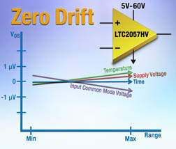
Another new op amp, the LTC2057 operates on a supply voltage of up to 60 V. It uses a zero-drift input topology to minimize changes over temperature, time, input common mode range, and voltage supply variation. It achieves 150 dB CMRR, which in our example would result in just a 1.60 µV error at the input, or 0.16 mV referred to the output.
The new LTC6090 is an example of an amp with an even wider common mode voltage range. Specified to operate on up to 140 V, its common mode input range extends to within 3 V of its rails. If we modify our example so that the 100 mV signal is riding on a common mode voltage ranging of 100 V, then the LTC6090, with a CMRR of 125 dB, would vary just 56.0 µV referred to the input or 5.60 mV on the output.
Choosing between these amplifiers will depend on other design considerations. The LT6016, mentioned above, includes many protection features, making it a great choice for applications where the inputs or outputs connect directly to the circuit board I/O. The amplifier is also unique for its ability to operate with its inputs well above the supply (up to 76 V above the negative rail).
And, the LTC2057 provides very wide dynamic range, with just 0.50 uV input offset voltage and the ability to operate with input signals within 1.5 V of a 60 V supply. Due to its zero-drift architecture, it also maintains its accuracy better than any other amplifier over changes in common mode voltage, temperature, time and supply voltage. The LTC6090, again from the above discussion, was designed for an extremely wide supply voltage range (up to 140 V) while providing accuracy almost as good as the LTC6016.
Advertisement
Learn more about Linear Technology


