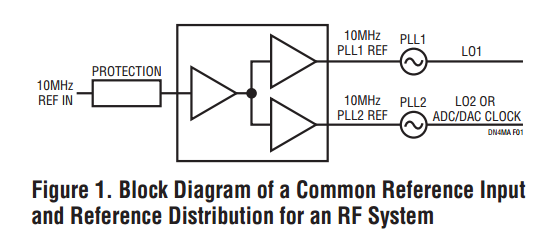
Designing the reference input circuit for an RF system can prove tricky. One challenge is maintaining the phase noise performance of the input clock while meeting the protection, buffering and distribution requirements for the clock. This article shows how to design a 10MHz reference input circuit and optimize its performance.
Click here for design note
Download full block diagram below
Advertisement

Learn more about Linear Technology


