Here are some principles to help you make the best design choices
BY ERIK MENTZE
Cypress Semiconductor
San Jose, CA
http://www.cypress.com
Configuring a phase-locked loop (PLL) for a given frequency synthesis application can be a quick and easy process or a time-consuming, tedious, and iterative process. And, after determining a set of frequency synthesis parameters for the system, there is always the doubt: Did I choose the best possible parameters? Perhaps there is a different set that will run cleaner and consume less power or have more margin? This article will attempt to shed some light on the principles behind the best design choices.
An overview of PLL frequency synthesis
At a fundamental level, the goal of any frequency synthesizer is, based on a given reference frequency, to generate a desired output frequency. They do so, usually, by dividing down the reference oscillator frequency and using a feedback loop with a phase detector to maintain phase coherence. Figure 1 shows the general form of a charge pump integer divide phase locked loop (a very common topology used for frequency synthesis).
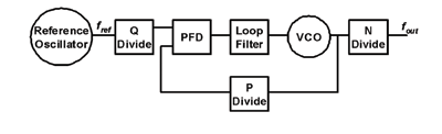
Fig. 1. Block diagram of a basic integer divide PLL.
The three divide blocks – the reference divider (Q), the feedback divider (P), and the output divider (N) – define the functionality of the loop and are chosen to set the desired output frequency. A common way of determining these values is to divide the output frequency by the reference frequency, and reduce the fraction:
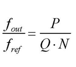
The difficulty in solving this equation is that there are three degrees of freedom and so the most common technique for solving it is to use a search algorithm. Such algorithms work by searching the solution space, looking for sets of P, Q, and N values that will result in the desired frequency result.
An additional configuration that is commonly used in programmable SoCs is to have multiple output dividers. This allows for the synthesis of multiple frequency outputs. Each output is an integer multiple of the VCO frequency. This topology emphasizes the importance of selecting the right VCO frequency so as to maximize the number of system clocks that can be generated off of the single PLL.
An example
For this example, we will synthesize a 50 MHz output from a 14.3181818 MHz reference (a common video frequency). Assume the VCO has a frequency range of 100 to 400 MHz. Using a search algorithm, we can determine the possible N divide values and use the corresponding VCO frequencies to determined Q and P values. All results for N values 2-8 are shown in Table 1. – a complete set of possible frequency synthesis parameters, given our reference and desired output frequencies.
|
N |
Fref |
|||||
|
[MHz] |
fvco |
|||||
|
[MHz] |
Fout |
|||||
|
[MHz] |
fpfd |
|||||
|
[MHz] |
Q |
P |
||||
|
2 |
14. 318… |
100 |
50 |
0. 227 |
63 |
440 |
|
3 |
14. 318… |
150 |
50 |
0. 682 |
21 |
220 |
|
4 |
14. 318… |
200 |
50 |
0. 227 |
63 |
880 |
|
5 |
14. 318… |
250 |
50 |
0. 227 |
63 |
1100 |
|
6 |
14. 318… |
300 |
50 |
0. 682 |
21 |
440 |
|
7 |
14. 318… |
350 |
50 |
1. 591 |
9 |
220 |
|
8 |
14. 318… |
400 |
50 |
0. 227 |
63 |
1760 |
Table 1. Summary of Example Results
Choosing an optimal configuration
Now that we have confidently found the set of frequency synthesis parameters, we can turn our attention to selecting the performance parameters. Several common parameters that are optimized in various applications are:
Power
Power is dominated by the VCO frequency, charge pump current, and divide block settings. Most VCO architectures require larger tail currents to achieve higher frequencies. So as frequency increases, so does power consumption. When larger charge pump currents are used (for loop stability or fast startup/settling time), more power is consumed per PFD period. Clock dividers dissipate power at each clock edge. Larger clock divide values require more divide cells to transition, consuming more power.
Startup time/settling time
The startup and settling time for a charge pump PLL is dominated by the loop natural frequency. This parameter can be thought of as the frequency slew rate of the PLL. It quantifies how fast the PLL can change the output frequency. It is proportional to the VCO gain and charge pump current, and inversely proportional to the feedback divide value and loop filter capacitance. Since the PLL output frequency is set by the VCO frequency, when we want to force a large step in the output frequency (either from zero at startup or from one setting to another) we need to force a large step in the VCO control voltage. This is accomplished by the charge pump dumping a large amount of charge onto the loop filter cap. The amount of frequency change/V increase on the loop filter is set by the VCO gain. The rate at which the loop filter voltage is updated is set by the PFD frequency.
Cycle-to-cycle jitter
Cycle-to-cycle jitter (the change in period length from one period to the next) can easily be dominated by the individual blocks of the PLL (VCO, dividers, reference oscillator), creating a situation where no loop parameter changes can improve performance. If you are working with a low noise PLL, then loop parameter settings can make a significant improvement.
Similar to startup/settling time, the PFD frequency and VCO gain play a key role. Higher PFD frequencies mean that the PLL loop filter voltage is refreshed at a higher rate. This prevents the loop filter voltage from drifting. By using a large loop filter capacitance, the amount of voltage drift per PFD period is minimized. Because the VCO gain dictates how far the output frequency drifts per unit voltage drift on the loop filter, lower VCO gain makes the PLL less sensitive to loop filter voltage drift.
Phase noise
Optimizing phase noise is highly application dependent, but a few general observations can be made. Phase noise contributed by the reference oscillator can be suppressed by setting the PLL to a lower closed loop bandwidth. Phase noise contributed by the VCO can be suppressed by setting the PLL to a higher closed loop bandwidth.
Phase noise divides down proportional to the output divide setting. If the output divider is a low noise divider, then running the VCO at a higher frequency and dividing the output frequency down will result in a phase noise improvement.
Optimizing the example
Finally, let’s apply this discussion on optimization.
Powe r. If low power consumption is the primary design concern we want to minimize VCO frequency and divide values. Selecting N=3, Q=21, P=220 would be the best choice. This operates the VCO at one of the lower frequencies, lower P and Q values, and has a reasonable PFD frequency.
Startup/settling time . If startup/settling time is the primary concern, then from Table 1 it is clear that the N = 7, Q = 9, P = 220 is the most desirable. It has an fPFD of more than two times any other configuration, resulting in a higher refresh rate on the loop filter voltage.
Jitter . If low jitter is the primary concern, then N = 7, Q = 9, P = 220 is again the most desirable. It has an fPFD of more than two times any other configuration, resulting in a higher refresh rate on the loop filter voltage and the lowest jitter of all the possible configurations.
Phase noise . Optimizing phase noise is highly application dependent and depends on specific reference oscillator and VCO noise performance. The one design choice we can make based on our configuration list is to choose a high VCO frequency that is divided down. N = 7, Q = 9, P = 220 is probably the best because its PFD frequency is so much higher than N = 8, Q = 63, P = 1,760. If the loop has high jitter, then the phase noise floor will rise significantly, swamping out any improvement the output divider is giving us. ■
Advertisement
Learn more about Cypress Semiconductor


