Types of FPGAs
The FPGA market is roughly divided into two types: flash-based logic arrays with nonvolatile memory cells, and SRAM-based FPGAs that hold their configuration patterns in static RAM memory cells. SRAM-based FPGAs require an external nonvolatile memory to hold their configuration pattern, which upon power-up is transferred via serial link into the SRAM-based device. In the past, the flash-based FPGAs trailed behind the SRAM-based devices in density, performance, and on-chip IP such as processor cores, high-speed I/O channels, and other functions requiring high density.
Benefits of Flash based FPGAs
Flash-based devices using advanced logic processes add performance and reduce power and cost. Advances in shrinking the flash memory cells and the ability to integrate the flash into advanced logic processes now let high-performance flash-based FPGAs deliver features and functions comparable to SRAM-based FPGAs, and often at a lower system cost. Additionally, the flash-based arrays often have a reduced system footprint and power consumption since an external configuration memory is not needed. Another benefit of flash-based devices is startup time — since the configuration memory is on the same chip as the logic, the configuration pattern loads almost instantly, whereas their SRAM-based cousins are still loading the configuration. This can be a critical feature in industrial, communications, medical, consumer, and other applications that must start or restart quickly.
Cost and speed
Flash technology has also transitioned from a specialty process to the mainstream, allowing flash-based FPGAs to compete in cost-sensitive markets while delivering logic densities of more than 150,000 logic elements (about 570 kgates). In addition, these FPGAs now offer dedicated digital-signal-processing blocks, high-speed SERDES ports capable of data-transfer speeds of multiple Gbits/s, PCIe serial interfaces, dedicated SRAM memory blocks, controllers for internal and external memory, and embedded security functions that prevent intrusion and allow secure data transmissions. Table 1 provides a short comparison of the features integrated into flash-based FPGAs vs. comparable density SRAM-based chips.
System requirements and design
For the midrange densities, designers have a wide choice of features, I/O pins, and package options to meet just about any system requirement. However, the various families each offer a different combination of features, so no one family solves every system need. This is especially true for the embedded-system support functions that help designers reduce complexity. On-chip functions such as PCIe endpoints, blocks of SRAM, DSP blocks (configurable multiplier-accumulator functions), and, of course, the programmable logic fabric are common to many flash- and SRAM-based FPGAs. However, unique functions such as embedded processors, memory controllers, multi-gigabit/s SERDES ports, and dedicated support for data encryption/decryption are more limited.
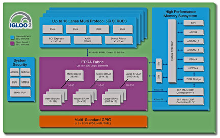
As Table 1 shows, there are many features in common among the three families, but where the families differ (aside from the flash or SRAM configurability), is in the quantity of I/O pins and the number of SERDES channels. Even though the flash-based FPGAs have many integrated functions, such as is illustrated by the architectural diagram of the IGL002 from Microsemi (see Fig. 1 ), the flash FPGAs can stand by and operate at lower power levels than the comparable SRAM-based devices.

Fig. 1: Packing many pre-integrated system-level support functions, the IGL002 from Microsemi is a prime example of what FPGA vendors can deliver.
Power consumption
In fact, power consumption in both active and standby modes can often be a deciding factor in FPGA selection, especially if the end system has to operate at low power levels or needs to run as long as possible on battery backup during a power outage. The flash-based devices offer many power-saving advantages vs. the SRAM-based FPGAs since flash FPGAs have zero inrush power and zero configuration power and can operate at a significantly lower active power than the SRAM-based FPGAs.
Security
Lastly, with the growing connectivity of systems, additional efforts must be taken to keep the systems secure against hacking as well as provide the ability to securely communicate with other systems through the Internet. However, once a system connects to the Internet, it becomes a target for hackers who might try to compromise the system by downloading new configuration data. To prevent that, FPGAs now include security subsystems that ensure only authorized configuration code or control programs are loaded and executed — this process is referred to as “SecureBoot.” Built-in countermeasures that prevent physical attacks such as antitamper and zeroization are available, and with flash-based FPGAs, keys and critical data can be kept confidential using on-chip secure flash storage.
BY FARHAD MAFIE
Vice President Worldwide Marketing
Microsemi, www.microsemi.com
Related articles:
Advertisement
Learn more about Microsemi


