Correct clock recovery for test synchronization
Extracting a clock from the data stream may be an obvious way to generate a synchronization signal, but doing so is nontrivial
BY GREG LECHEMINANT
Measurement Applications Specialist
Agilent Technologies
www.agilent.com
Many common measurements require some form of timing reference to synchronize the measurement process. While synchronizing clocks are often available directly from a test system, functioning communications networks may need to be tested where no clock signal is present. Extracting a clock from the data stream is an obvious way to generate the required synchronization signal.
By reviewing the basics of clock recovery and various test scenarios that employ it, we can discover important details on how to understand and correctly interpret measurement results when using recovered clocks.
High-speed digital comm
In high-speed digital communications, where accurate signal characterization is a must, time-domain waveform analysis is an integral part of assessing transmitter performance. Edge speeds, eye amplitude, and timing jitter are examples of common parameters engineers need to observe.
Communications industry standards require similar measurements to guarantee communications quality. For troubleshooting and characterizing system-level performance, real-time oscilloscopes with bandwidths exceeding 60 GHz are the primary tool. For the chipsets and components used in both optical and electrical digital communications, “equivalent-time” sampling oscilloscopes (often simply called sampling scopes) with bandwidths to 100 GHz are commonly used to achieve the most accurate measurements. Clock recovery is available for both oscilloscope technologies.
A scope requires a reference signal, commonly called a trigger, to anchor the time axis of any measurement. For eye-diagram measurements, this should be some form of clock signal that is synchronous to the signal being observed. When measuring transmitters in a laboratory environment, this synchronous clock signal is usually available from the test setup.
However, when the transmitter is integrated into a communications system or bus, the data signal itself may be the only signal present. In this situation, a synchronizing signal for triggering may be derived from the data stream through some form of clock extraction. While the extracted clock solves the need for a triggering signal, it can also significantly alter the displayed waveform compared to triggering with the direct clock signal. Transmitter timing characteristics, such as jitter the deviation of the significant instants of a signal from their ideal positions in time are important in a high-speed system. If excessive, jitter can result bit errors seen as closure of the “eye” in a scope-displayed “eye diagram.”
Scopes display signal amplitude versus time, where time is defined relative to the signal triggering the scope. If the oscilloscope is triggered with a jitter-free or “clean” clock signal, the waveform timing performance is relative to this clock signal. If the triggering clock represents ideal timing positions, data edges will be seen as advanced or retarded from their ideal positions, if they are advanced or retarded relative to the triggering clock.
On the other hand, if the triggering signal is derived from the data to be observed, it becomes complicated to interpret what the jitter performance is. In effect, the signal is being compared to itself. In this scenario, one might observe displayed signals to be completely absent of jitter, even if there is significant jitter when the signal is observed with a jitter-free reference clock. The effect is similar to what is observed when the oscilloscope is triggered on the data stream directly, as is common with a real-time oscilloscope.
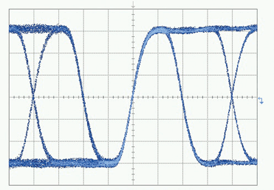
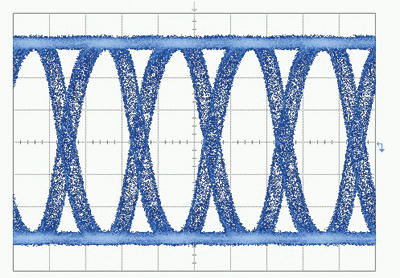
Fig. 1: An eye diagram of a “jittery” signal is seen with the data signal as the scope trigger (left), and with a ‘clean’ jitter free trigger (right).
The two waveform displays of Fig. 1 are of the same signal. The difference between the two is due simply to how the oscilloscope was triggered.
The oscilloscope is configured to display the triggering event at the center of the screen. When triggering on the data (left waveform), note that at “0” time the eye diagram is incomplete. This is due to the oscilloscope being set to trigger on rising edges only. No jitter is observed here because the ideal edge position is defined by the trigger event, which is from the signal being observed.
While the signal appears to be jitter free, in this example approximately 0.25 unit intervals of jitter (25% of the bit period) was intentionally impressed upon the data stream. This is observed when the oscilloscope is triggered with a jitter-free clock (right waveform).
Two important points are borne out in the above waveforms. First, if one wishes to see all the jitter present on a signal, the scope must be triggered with a signal that represents the jitter-free condition. Using such a clock signal could prove useful in characterizing how much jitter a circuit adds to a pristine signal from an instrumentation-grade pattern generator. The ideal triggering signal would then be the pattern generator clock output.
Second, if the oscilloscope is triggered with a signal that contains jitter that is also present on the signal being observed, the “common” jitter may not be displayed. In this case, the jitter observed when the oscilloscope is triggered with a clock signal derived from the data will be dependent upon the spectrum or frequency range of the jitter present on the signal. It will also depend on the design of the clock extraction system.
Clock extraction circuits
Clock extraction circuits are typically based upon a phase-locked-loop (PLL) structure (see Fig. 2 ). The voltage controlled oscillator (VCO) is phase locked to the incoming data stream and will run at the same rate as the input signal. If the data rate fluctuates, an error voltage proportional to the change in data rate will be generated by the phase detector and will cause the oscillator to shift in frequency and “follow” the data.
Adjusting the loop gain in the PLL structure will control how fast and how far the incoming data can deviate from its nominal rate while maintaining tracking with the VCO. This is sometimes referred to as the PLL loop bandwidth or jitter transfer function (JTF):
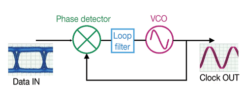
Fig. 2: A clock extraction circuit based on a PLL locks a VCO to the incoming data stream.
The basic open-loop equation for the PLL A(s) is dependent on the rate at which the incoming data signal deviates from its ideal. In other words, if the data has low-frequency jitter, the gain is high, but diminishes as the jitter frequency increases. With the loop closed, the response becomes:

Equation 1 describes the JTF, the amount of jitter that will be present on the recovered clock (VCO output) relative to the jitter on the incoming data stream. This function generally has a low-pass effect. That is, JTF is at unity over low frequencies, but as the jitter increases to higher frequencies, the jitter on the recovered clock will decrease in magnitude. The JTF or loop response for the closed loop gain is shown in the blue trace of Fig. 3 .
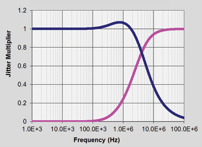
Fig. 3: Jitter transfer (blue) and resulting observed jitter transfer function (pink) for a PLL loop used to trigger an oscilloscope.
The jitter transfer response shows the amount of jitter that will be present on the recovered clock, relative to the jitter on the incoming data, as a function of the jitter frequency. If this signal will be used to trigger an oscilloscope and observe the original data signal, the jitter transfer plot provides some insight into what jitter can and cannot be observed on the displayed waveform. The resulting transfer function for the jitter observed on the displayed waveform (observed jitter transfer function or OJTF) is:

Intuitively this can be understood as the effect of jitter being common to both the data observed and the triggering signal. As long as the jitter frequency is within the PLL’s loop bandwidth, the jitter observed on the data stream, relative to the oscilloscope time reference (the triggering signal) is zero. While the JTF of the PLL has a low-pass characteristic, the OJTF follows a high-pass response.
When jitter is at low frequencies, the OJTF function is zero. At high-jitter frequencies the OJTF function goes to unity. In Fig. 3, note that in this specific case, while the JTF response of the PLL hardware has some gain above unity before rolling off, the OJTF has a very well behaved response. It is also possible for the reverse to be true. Peaking is common with multiple-pole PLL designs.
Jitter transfer
Historically, the term “jitter transfer” has been used to describe the loop bandwidth of the PLL or a system repeater. Some recent communications standards have used “jitter transfer” to describe the jitter that is ‘transferred to the displayed waveform’ when clock recovery is used to trigger the oscilloscope. Unfortunately these two definitions of “jitter transfer” are the mathematical complements of each other. The term “observed jitter transfer” is preferred to describe the jitter seen on the oscilloscope.
Another complication occurs when “software” clock recovery is used with real-time oscilloscopes. Sampling oscilloscopes use actual PLL hardware to create a clock trigger. The real-time oscilloscope can acquire a very long time record, including hundreds to millions of bits. Through post-processing, an effective clock signal can be derived from the waveform and the waveform record can be displayed relative to the virtual clock. This clock signal can also be filtered in software to mimic the effect of the PLL bandwidth. However, when defining the filter bandwidth, the high-pass OJTF frequency corner is set rather than the low pass bandwidth of the PLL JTF.
Note that the OJTF response is not a simple complement of the loop response. The JTF response is complex and phase must be considered. The 3-dB bandwidth of the jitter transfer low-pass response is not necessarily at the same frequency as the 3-dB bandwidth of the observed jitter transfer high-pass response. This leads to some important points regarding the use of hardware clock recovery systems used to trigger a sampling oscilloscope versus software clock recovery used to process and display the waveform acquired by a real-time oscilloscope.
All other things assumed to be equal, the OJTF achieved by setting the loop bandwidth of the hardware clock recovery is not necessarily the same OJTF achieved by setting the bandwidth of the software PLL. Also, sampling oscilloscopes have a significant delay between the time when the instrument is triggered and when a data sample is taken. The minimum delay is typically on the order of 20 ns. This alters the OJTF function, with an effect similar to peaking and some oscillation, but can be eliminated, and is discussed later.
Using an extracted clock to trigger an oscilloscope is a strategy used in several communications standards to eliminate low-frequency jitter in transmitter waveforms. Since receivers used in communications systems have their own PLL’s to generate receiver clocks and can track out jitter, transmitters should not be rejected for low-frequency jitter, even if the jitter is large. Achieving expected results requires a thorough understanding of recovered clock triggers. Well-engineered instrumentation can simplify the process.
Recent developments in hardware clock recovery instrumentation allow clock triggers to be extracted from signals at any data rate from 50 Mbits/s to 32 Gbits/s. The clock recovery circuitry can be a standalone instrument, or it can be integrated into the oscilloscope. To remove the effects of oscilloscope trigger-to-sample delay of the sampling oscilloscope, the delay term is effectively forced to zero. How this is achieved depends on whether the clock recovery hardware is integrated into the oscilloscope or if it is a standalone instrument connected to the oscilloscope.
A zero trigger-to-sample delay can be achieved if the signal path to the oscilloscope input (after clock extraction) has delay equal to the inherent trigger-to-sample delay of the oscilloscope. When performing optical measurements, this is easily achieved by placing a length of fiber (path length equivalent to the delay) in the signal path. For electrical measurements, extra cable can be added, but, depending upon the frequency content of the signal and the quality of the cabling, will likely impact the fidelity of any waveform measurements.
When the clock recovery circuitry is integrated into the oscilloscope system, a high-integrity pick-off delivers a small portion of the incoming signal to the PLL while the main signal goes to the sampling electronics. The recovered clock is used to trigger the sampler and determine the amplitude of the test signal. However, the clock is also routed to a precision timebase (PTB) section.
The PTB is triggered at the identical time as the sampler and is used to determine the time at which the amplitude sample was acquired. Because there is no delay between the triggering of the sampler and the triggering of the PTB, the effective trigger-to-sample delay is zero. No signal-degrading cabling is required. An additional benefit of having the PTB and clock recovery hardware integrated into the oscilloscope is the residual jitter of the measurement system is reduced to well below 50 fs.
Residual measurement errors due to a nonideal OJTF are systematic. Thus post-processing of the measurement results can remove jitter measurement error caused by imperfections in the instrumentation hardware. In fact, when the clock recovery hardware is integrated into the oscilloscope, the overall system JTF, and perhaps more importantly the OJTF, can be displayed and controlled by the user assuring expected results (see Fig. 4 ).
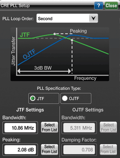
Fig. 4: Complementary control of JTF and OJTF assures expected results
Receiver emulation
Loop bandwidth control also provides the ability to emulate the behavior of system-level receivers. The jitter observed on the oscilloscope will be similar to the jitter that a decision circuit must tolerate if the clock recovery design of the instrumentation matches that of the receiver. Adjusting the order and bandwidth of the clock recovery and its impact on the observed jitter of a transmitter signal provides insights into the ideal design of PLL’s used in receivers.
The phase detector of the hardware clock recovery system acts as a jitter demodulator. If the phase detector output is monitored, the jitter present on the incoming signal can be directly observed. Transforming the extracted jitter signal into the frequency domain results in an effective jitter spectrum analyzer. Observation of the discrete tones of the jitter spectrum can allow direct identification of sources of jitter (Fig. 5 ). Receiver designs can be optimized with knowledge of the jitter spectrum of the transmitted signal. This is possible with both integrated and external hardware clock recovery.
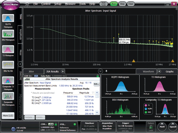
Fig. 5: The jitter spectrum of the data signal provides insight into root causes of jitter.
Clock recovery instrumentation provides an important method to synchronize and trigger oscilloscopes for measurements of high-speed digital communications signals. Precise control of the loop bandwidth properties allows important control over the jitter that is filtered and what is observed. Integration of clock recovery hardware within a sampling oscilloscope provides the highest fidelity and easiest control for electrical waveform analysis and provides better correlation between sampling and real-time oscilloscopes. For optical test, signal integrity is easier to maintain and external clock recovery solutions are often more flexible. ■
Advertisement
Learn more about Keysight Technologies, Inc.


