BY MIKE RESSO, Signal Integrity Application Scientist, and HEIDI BARNES, Senior Application Engineer
Keysight Technologies, Inc.
www.keysight.com
USB 3.1 Gen 2 Type-C — which will mean quicker data transfer rates (2.5 times quicker), faster charging (up to 100 W), and, thanks to the smaller connectors, even smaller consumer electronics — is just now being adopted by manufacturers. It will take at least a couple of years for Type-C to be considered the “universal” option and, to become that, today’s designers of high-speed digital devices will need advanced equipment and software to characterize and model the Type-C physical layer channel.
USB Type-C is one of the more challenging architectures for digital design engineers due to the extreme rise time of the digital signals it’s meant to carry. This, combined with the small physical size of this high-density reversible connector, increases the risk that design engineers will encounter unforeseen interoperability issues at the fundamental, physical layer. These issues can be avoided by leveraging measurements and simulations to adequately debug and characterize the performance-controlling interconnect features and fabrication tolerances.
This article discusses a step-by-step process that signal integrity engineers can follow to ensure their success in designing with USB Type-C devices. It deals with the basics of simulation/test, including some tips and techniques for dealing with S-parameters.
How does USB Type-C compare?
One easy way to increase electrical performance is to make things physically smaller. The shorter electrical delay through a typical non-homogeneous dielectric system, such as a printed circuit board micro-strip transmission line, will, by its nature, have less loss than a physically longer device. In this way, the USB Type-C connector, which is smaller than other commonly used consumer connectors, can contribute to lower loss and higher bandwidth.
At the same time, higher densities create new challenges in maintaining transmission line impedances through connectors and onto a PCB while avoiding crosstalk and EMI problems. Consider a USB Type-C receptacle fixture and a USB Type-C Plug fixture (Fig. 1 ). At 10-Gbps data rates, there can be multiple 100-ps-wide bits occupying the path between transmitter and receiver. Any impedance problem in the path will, with each rising and falling edge, result in a multiplicity of reflections and coupling. The multiple reflections can make it difficult to debug the full link connection.
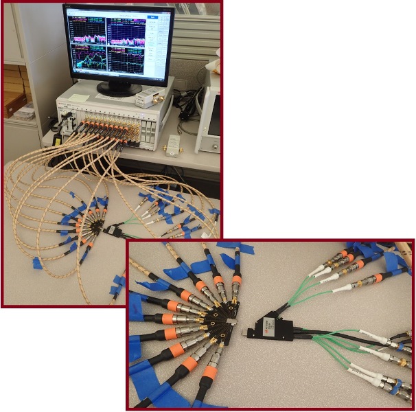
Fig. 1: The test configuration shown here uses a set of 10 two-port PXI VNA cards along with two special test fixtures shown in the inset. The fixture on the left, dubbed “lux,” is a USB Type-C receptacle fixture, while the one on the right, called “n70515a,” is the USB Type-C plug fixture.
To simplify the debug process, it is important that an engineer can simulate and measure each component in the USB physical layer link and thereby determine which one is not meeting performance requirements. Typically, advanced measurement-error-correction techniques must be used to accurately de-embed the test fixtures from the measurement of a USB Type-C host, device, or cable. Furthermore, modeling and simulation also benefit from accurate measurements of the components for improved simulation-to-measurement correlation that can help mitigate complications due to challenging physical layer structures.
How is the physical layer measured?
Linear passive interconnects, such as those found in a USB Type-C physical layer, are typically characterized with two types of stimulus/response test instrumentation: in the time domain, the time domain reflectometer (TDR); in the frequency domain, the vector network analyzer (VNA). Whether the native instrument gathers time or frequency domain data, one domain’s data set can be transformed into the other’s by straightforward mathematics (such as the Fourier transform or the inverse Fourier transform); specialized signal integrity software (such as Keysight’s Physical Layer Test System, or PLTS software) exists to provide ease of use to digital and microwave engineers alike to accomplish this domain transformation.
While most signal integrity applications can be addressed with a basic four-port measurement (two ports in and two ports out), there are some advanced tools that make the job easier and present additional insight into the performance of the device under test (DUT). This is the case with the 20-port PXI-chassis-based VNA we used; a 20-port data set measurement for this USB Type-C channel took just over two minutes.
The vast amount of data gathered in this fashion was stored as a standard format Touchstone file, which can subsequently be imported into SI specialist software for analysis. A 20-port measurement yields a 20 x 20 matrix of S-parameters with over 400 plots in a single domain. Multiplying this by the number of domains (time and frequency) and topologies (single-ended or differential) possible produces a massive amount of data. Attempting to manage this amount of measurement data manually is a nightmare, but it can be easily handled with the aforementioned PLTS software.
When properly analyzed, this metadata set can produce insight into the high-speed digital channel as never before. Differential insertion loss, differential return loss, impedance profile, eye diagram, near-end and far-end crosstalk, mode conversion, and channel optimization with pre-emphasis and equalization can be characterized fully.
Tips and techniques for quality measurements
As seen in Fig. 1 , the VNA setup consists of a Peripheral Component Interconnect Extension (PCI-X) chassis with modules that slide in and out for scalable test capability. One embedded controller and 10 VNA modules (each module being a two-port VNA) produces a 20-port VNA. The VNA modules measure from 300 kHz to 26.5 Hz and provide excellent speed, high dynamic range, low trace noise, and persistent stability to improve accuracy of the USB Type-C measurement.
The test cables fan out to the channel under test — in this case, a USB Type-C receptacle test fixture and a USB Type-C plug assembly. The blue tape on the end of each test cable is meant to stabilize the test cables for added calibration accuracy. The calibration used is the Unknown Thru method (also referred to as the Reciprocal Thru method), and the tape ensures that the cables are not moved between calibration and measurement of the DUT. This is a well-known tip that can minimize phase-shift in sensitive calibrations to achieve the utmost accuracy.
Another helpful tip when making multiport measurements is to spend some time to logically label each port of the S-parameter data set. Next, it helps to remap the ports so that analysis software can easily use default
1-to-2, 3-to-4 channel topology for direct plotting of mixed-mode parameters (Fig. 2 ). Having an SI tool that makes it easy to visualize the single-ended and differential port mapping and re-order if needed is a great time-saver when working with large data sets.
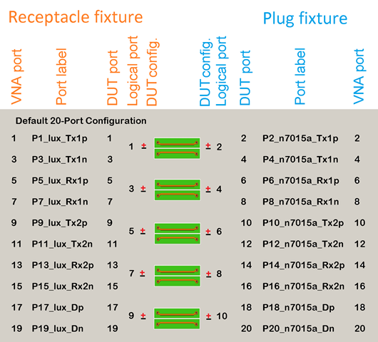
Fig. 2: Type-C supports data transmission paths for both USB 2.0 (Dp and Dn) and USB 3.1 (Transmit — TX1p, TX1n, TX2p, TX2n — and Receive — RX1p, RX1n, RX2p, RX2n). Clearly mapping the ports of the VNA to the fixture and DUT ensures that the analysis will be fully understood in terms of the DUT’s performance.
Differential S-parameters
The USB physical layer uses differential signaling that can contain a significant mount of coupling between the p (+) and n (−) paths of the differential pair. This requires the use of mixed-mode parameters to correctly analyze the performance of the Tx and Rx channels. As a quick S-parameter refresher, Fig. 3 shows the 4 x 4 matrix of mixed-mode S-parameters. Interpreting this 16-element S-parameter matrix is not trivial, so it is helpful to analyze one quadrant at a time.
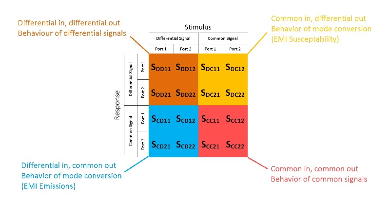
Fig. 3: Each quadrant of a measured S-parameter matrix has much to tell about the performance of the DUT when compared to the ideal matrix.
The first quadrant in the upper left is defined as the parameters describing the differential stimulus and differential response characteristics of the device under test. This is the actual mode of operation for most high-speed differential interconnects, so it is typically the most useful quadrant and is analyzed first.
The fourth quadrant is located in the lower right and describes the performance characteristics of the common signal propagating through the device under test. If the device is designed properly, there should be minimal mode conversion and the fourth quadrant data will be of little concern. However, if any mode conversion is present due to design flaws, then the fourth quadrant will describe how this common signal behaves.
Located in the upper right and lower left of Fig. 3 , respectively, the second and third quadrants are, in the authors' opinions, the most interesting quadrants for engineering analysis. These are also referred to as the mixed-mode quadrants because they fully characterize any mode conversion occurring in the device under test, whether it is common-to-differential conversion (EMI susceptibility) or differential-to-common conversion (EMI radiation). Understanding the magnitude and location of mode conversion is very helpful when trying to optimize the design of interconnects for gigabit data throughput.
Click here to read Part 2.
Advertisement
Learn more about Keysight Technologies, Inc.


