In Part 1 of this article, we gained an understanding of the fundamental idea behind differential S-parameters. Now we can begin to explore the vast amount of information inside the multichannel Touchstone file (Fig. 1 ). While at first seemingly complex, there are basic methods of analysis that can be done time and time again with very successful results. We will now discuss some of those analysis tips and techniques that can help to provide the quickest path to the insight of the device performance.
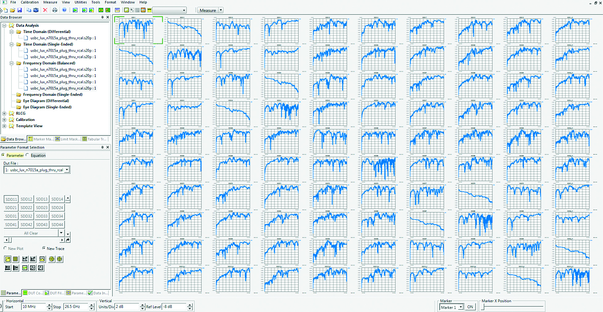 Fig. 1: In an upper left quadrant of the 20-port .s20p Touchstone file, 400 S-parameters can be viewed one at a time or with multiple plots at a time.
Symmetry is a beautiful thing
One of the first steps in the analysis of large, multichannel S-parameter files is to use the time domain. VNA S-parameter measurements can be modified with an Inverse Fast Fourier (IFFT) function to extract the TDD11 time domain parameter, which is the impedance profile described as resistance versus time, with time representing distance (the time it takes for the signal to travel to and reflect from a resistance change, or discontinuity).
Why is this preferred over using the SDD11 frequency domain data? Because the frequency domain does not provide any spatial information. In the time domain, the location of bad cables, opens, shorts, and other anomalies can be quickly located. Plotting differential impedance profiles of all of the differential channels is a quick way to conduct this type of “sanity check” of the measurement set-up before saving the data.
A plot of all of the differential channels (Fig. 2 ) shows a beautiful symmetry between all of the forward and reverse impedance profile waveforms. There should be a multitude of mirror image waveforms because we have automatically measured each channel forward and reverse. This is the benefit of having a high-port-count instrument.
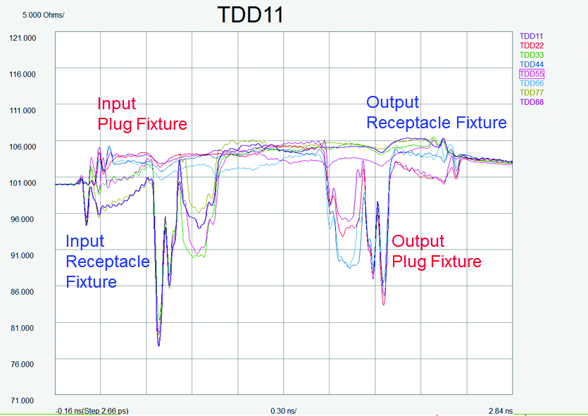 Fig. 2: A plot of all of the differential channels shows a beautiful symmetry between all of the forward and reverse impedance profile waveforms.
The waveform legend in the upper right indicates that we have plotted TDD11 through TDD88. TDD11 is the forward differential impedance profile of the same exact channel as TDD22, except TDD22 is just the backward differential impedance profile. So these two measurement plots should be symmetric, and they are. The same is true for the remaining plot pairs.
Forward and reverse channel impedance profiles
The next step in analyzing the data channels is to spatially locate the USB Type-C connector in the middle. (We know that it is somewhere near the middle, but the exact location is really needed.) To do this, we again look to the time domain data and simply measure the channel after we have physically disconnected the two fixtures. When we disconnect the two fixtures, we will see the impedance profile of one fixture terminated into an open circuit. This is indicated with a sharp vertical line going straight up to infinite impedance at the location in time where the connector is located (Fig. 3 ).
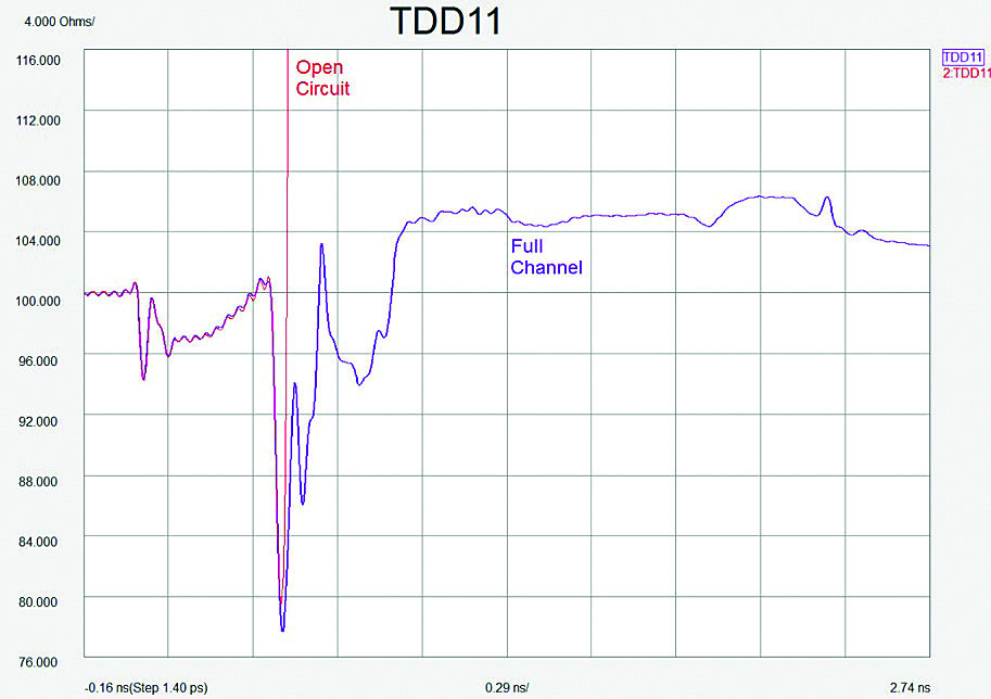 Fig. 3: The vertical red line represents the open circuit while fixtures are disconnected. This gives insight into where each fixture ends and begins.
To validate and double-check our work, we will look at the same impedance profile of the disconnected fixtures, but now looking from the other direction (Fig. 4 ). As we mentioned previously, the TDD22 is just the backward impedance profile of the TDD11 channel. We see the same vertical red line indicating exactly where one fixture ends and the other begins. It is obvious in looking at these last two TDD11 and TDD22 waveforms that the two fixtures are quite different from each other.
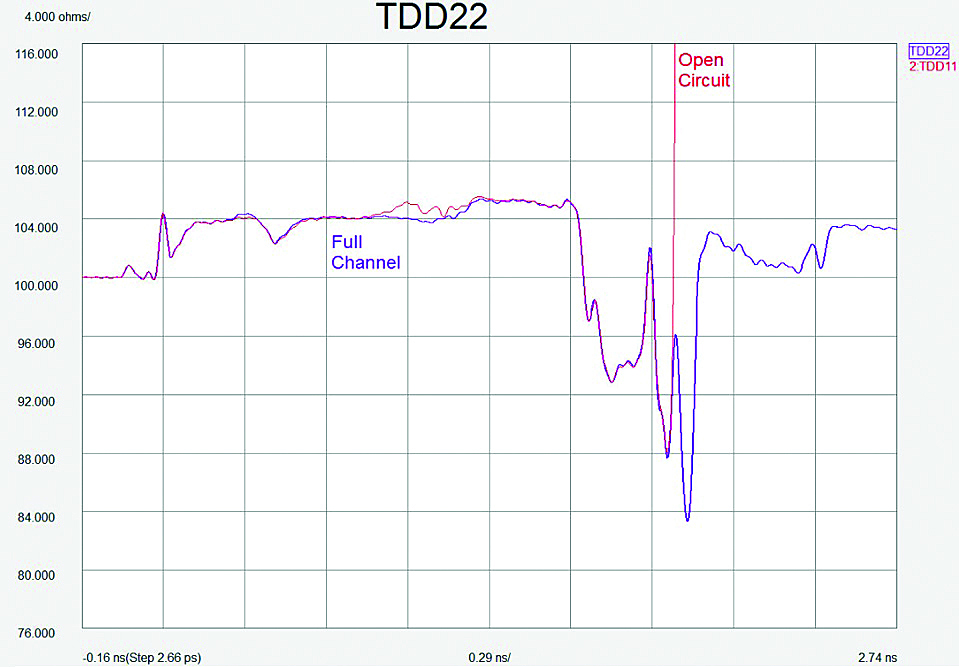 Fig. 4: Comparing this figure with Fig. 3 shows how different the fixtures are from each other.
The measurement channel
Historically, there have been two methods commonly used to remove the effects of the measurement fixture from the device under test, or DUT (Fig. 5 ). 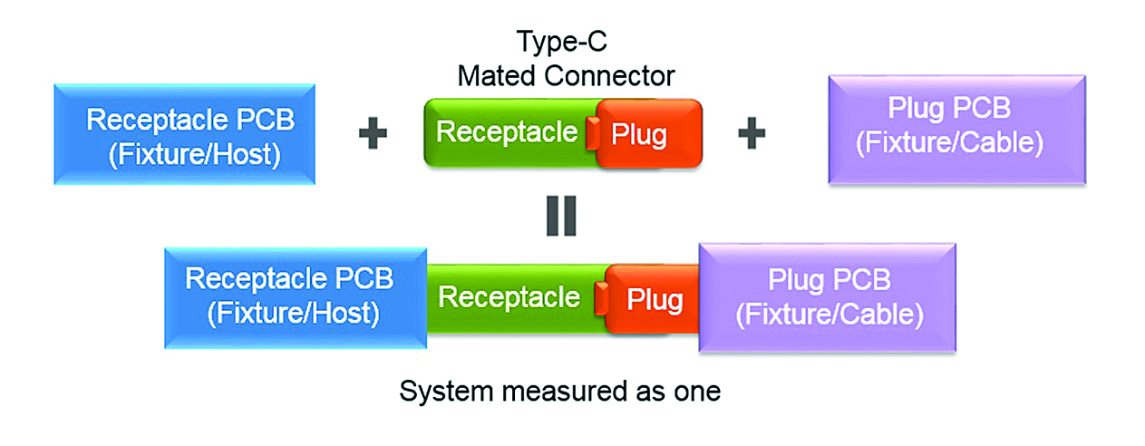
Fig. 5: To accurately measure the device under test (DUT), the effects of the fixtures must first be removed.
The first method is to model the fixture using an electromagnetic simulator and use the S-parameter results of the simulation to de-embed the effects of the fixture. It can take some time to create an accurate model for the fixture. The second technique is to build calibration standards on the same PCB used to fabricate the fixtures.
These traditional methods of calibration place the reference plane on the fixture PCB at a location where custom standards can be placed. Calibration standards like TRL require a TEM mode at the reference plane; that is, the mechanical structure is mirrored across the reference plane. The end result of this type of calibration typically leaves the mated connector performance as a part of the DUT, such as a USB host, cable, or device. The fixture can be removed from the full-path measurement to get the S-parameters of the DUT that includes the mated connector performance (Fig. 6 ). This is often desired because the vendor of these different components in a channel needs to show that their product will work with the mated connector. Fig. 6: While the fixture can be removed from the full-path measurement to get the S-parameters of the DUT that include the mated connector performance, what type of calibration will place the reference plane in the middle of the mated connector to provide the correct channel delay?
But while including the mated connector in the DUT works great for characterizing and comparing the performance of different components in a channel, it creates challenges when cascading components together in simulation for comparison with measured full-path performance. To the observer, it looks obvious that one should split the mated connector at the mating surface, and leave only the plug or receptacle as part of the DUT. The difficult question is, what type of calibration will place the reference plane in the middle of the mated connector?
Automatic fixture removal
A relatively new technique introduced a couple of years ago, called Automatic Fixture Removal (AFR), requires only one calibration standard, not the multiple standards required for TRL. That standard can be a back-to-back 2x fixture through path or, in some cases, just an open 1x fixture structure. The through is simply the left half and right half fixtures connected without a DUT. The big assumption here is that the through has to be symmetrical. In the case of the USB Type-C connector, it is difficult to create a back-to-back through path, since a receptacle cannot mate to another receptacle.
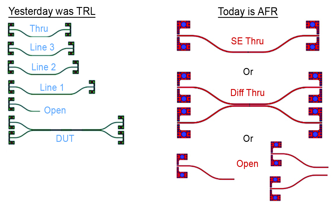
Fig. 7: Comparing traditional TRL calibration structures (left) and those used by AFR technique (right), the AFR applies a second-tier AFR calibration to move the measurement reference plane to the final location.
The 1-Port AFR technique has the advantage that it is able to automatically place the reference plane at the desired mating surface of the Type-C plug and receptacle (Fig. 8 ). This results in an S-parameter behavioral model of the host, cable, or device that can be cascaded in a simulation, thereby improving the simulation-to-measurement correlation with accurate electrical delays.
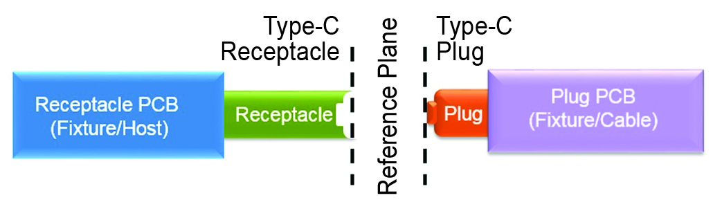
Fig. 8: The 1-port AFR technique automatically places the reference plane at the mating surface of the Type-C plug and receptacle.
The electrical delay of each components can be measured with either group delay in the frequency domain or the arrival of the impulse response peak in the time domain (Fig. 9 ). The 1-port AFR measurement of the plug fixture time delay and the receptacle fixture time delay add up to the measured full path time delay of the two fixtures plugged together.
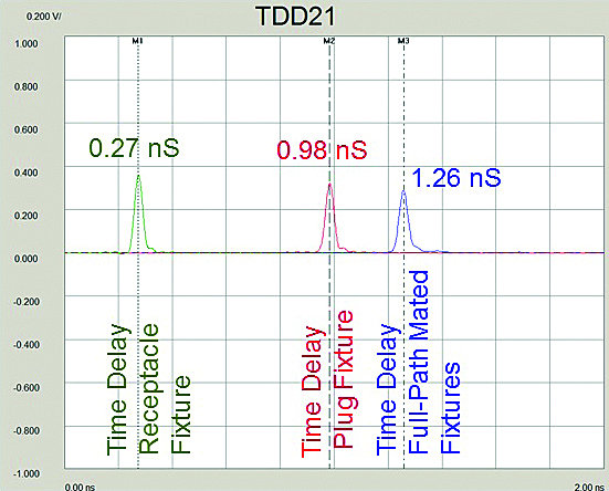
Fig. 9: The 1-port AFR measurement of the plug fixture time delay and the receptacle fixture time delay add up to the measured full path time delay of the two fixtures plugged together.
Advertisement
Learn more about Keysight Technologies, Inc.


