Cost effectively meeting energy-efficiency targets
Increased efficiency and lower BOM costs from premium power-semi components can offset new complex converter topologies
BY JOHN JOVALUSKY
Qspeed, Santa Clara, CA
http://www/qspeed.com
Despite the present economic reprieve, global energy consumption is increasing faster than new sources of power can be put into service. Trying to reduce the rate at which electrical power demand is growing, local and regional governments are setting increasingly higher efficiency standards for a growing list of products that use electricity.
For example, in November 2009, the California Energy Commission (CEC) announced that effective January 1, 2011, televisions with screens of up to 58 in. must meet new efficiency requirements to be sold in the Golden State. This means that power supply engineers must find new ways to improve the efficiency of the power conversion circuitry they design.

A 12mm-thick 300-W non-interleaved CCM boost converter stage for flat screen TV applications (>95% efficient at 120 Vac).
New standards requirements
Most of the new efficiency standards are similar to those developed by the U.S. Environmental Protection Agency’s (EPA) Energy Star program, which have generally followed the mandatory regulations that have been established by the CEC. Prior to the new standards, power supply efficiency was typically only specified and measured at full load. However, most power supplies rarely operate at full load, and may spend much of their time unloaded, or at very light loads (10% to 25%).
The researchers who developed these standards began by measuring the efficiency of many commercially available power supplies to establish baseline performance. During testing, they discovered that the efficiency of most of the power supplies they evaluated was poor at light loads.
They also observed that many of the power supplies had fairly high values of no-load power consumption. Since their goal was to mitigate power demand growth, many of the new standards addressed no-load power consumption in addition to setting minimum efficiency targets for multiple operating points.
The new standards specify minimum efficiency levels for several load points, such as 20%, 50%, and 100% in the 80 Plus computer power supply program, and 25%, 50%, 75%, and 100% in the CEC and Energy Star specifications for External Power Supplies (EPS). Maximum no-load power consumption levels also are specified in the EPS standards. Lastly, EPA Energy Star added minimum power factor (PF) specifications (0.9) for computer power supplies that went into effect in July 2009.
Meeting efficiency demands
To meet these requirements, designers have resorted to new strategies for improving the efficiency of the power supplies they design. For example, many engineers had realized that they could meet the harmonic-current specifications of specs such as IEC61000-3-2 with filtering alone.
However, ensuring that full-load PF is >0.9 requires the use of an active power factor correction (PFC) pre-regulator, which is most cost effectively implemented as a boost converter. Initially, active PFC converters were used in power supplies of 300 to 1,600 W, as a cost-effective way to ensure that they complied with the harmonic current requirements of IEC61000-3-2. However, well-designed boost converters can operate very efficiently (>95%) and can enable more efficient operation of the downstream output converter stage, since it can be optimized to operate from a fixed, high input voltage.
Switched-mode converters can be designed to deliver their full-load power while operating in the continuous conduction mode (CCM) or the discontinuous conduction mode (DCM). From a bill-of-materials (BOM) cost perspective, DCM active PFC boost converters tend to be less expensive solutions for power supplies that must deliver a maximum load power of around 200 to 250 W. Above 250 to 300 W, CCM operation tends to provide the more cost-effective solution. This is an important crossover range because a CCM boost converter requires a better performing and more expensive diode than does a DCM converter. Additionally, a CCM stage will require different EMI filter components to ensure that it meets conducted emissions limits than will a DCM stage.
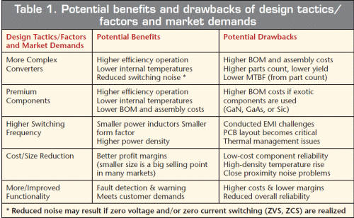
Table I shows the benefits and drawbacks of the design tactics, factors and market demands that influence the business decisions power supply manufacturers must make. Of these tactics and factors, the one that often offers the highest improvement in converter efficiency for the lowest cost is still the use of premium components; particularly, the best available power-semiconductor devices.
Table 1. Potential benefits and drawbacks of design tactics/factors and market demands

Important specs
In switched-mode converters, the greatest loss quadrant for all power rectifier diodes — bipolar or Schottky is forward conduction, with the forward-voltage drop (VF ) being the dominant factor. That is what prompted the use of MOSFETs as synchronous rectifiers, in low-voltage output rectification applications, since their on-state drain-to-source voltage (VDS ) is substantially lower than the VF of any rectifier diode.
However, a number of technical issues prevent that same tactic from being used to replace the boost diodes used in active PFC converters. Schottky diodes, made from silicon carbide (SiC) or gallium nitride (GaN) are the latest attempt to improve CCM boost converter efficiency. However, those diodes are still prohibitively expensive for cost-sensitive applications. As a result, several power-semiconductor manufacturers have introduced improved ultrafast, bipolar silicon diodes in the past few years.
The second greatest loss quadrant for power diodes is the turn-off transition. During forward conduction, the cathode of a bipolar device is saturated with minority carriers (holes) injected into it by the anode. Those carriers must be cleared from the cathode before a depletion region can develop to withstand the reverse voltage.
Those carriers are considered stored charge (called QRR for bipolar devices), since they must be evacuated from the device before reverse blocking can occur. QRR is removed by two mechanisms: (1) the holes recombine with electrons at designated “recombination centers” that are strategically located near the anode, and (2) they are swept back into the anode and out of the diode as reverse recovery current (IRR ).
Because adding recombination centers increases the VF of the device, QRR and IRR cannot be eliminated but only minimized. In a boost converter, the diode location and the high output voltage make the effects of diode IRR all the more detrimental to efficiency because IRR flows through the boost MOSFET as it is transitioning through its active region, where power dissipation is quite high.
Since the QRR of a boost diode determines the IRR that flows through it, each time the diode is switched off which can reduce the efficiency of the converter by 1% to 2% then the datasheets of those diodes ought to specify maximum values for QRR and/or IRR . However, most boost diode datasheets only specify typical values for those parameters, if they are specified at all.
This is usually the case because QRR and IRR are not easy to measure and every test that is performed on each part increases its cost. Therefore, if a datasheet only contains typical values for these parameters, chances are they were obtained from device characterization, and are not measured on, nor guaranteed for each part.
Qspeed Semiconductor was the first manufacturer to specify and test the QRR of every diode it ships. Qspeed’s new H-Series family of 600-V diodes is optimized to have the lowest QRR (even at junction temperatures of 125C) of any bipolar, silicon diodes available.
Before design engineers decide to try out a new, complex converter topology, they should consider the increased efficiency and lower BOM cost benefits that can result from using premium power-semiconductor components in their present designs. ■
Advertisement
Learn more about Qspeed Semiconductor


