Design considerations for the various output current levels, brief noise considerations, and voltage compliance problems
BY NICHOLAUS W. SMITH
Integrated Device Technology
www.idt.com
A current source is a critical component in most integrated and discrete circuits and can be described as an electric circuit that generates a steady flow of electrons for a given period of time no matter what load impedance it is driving. Now the part that makes the current source interesting is that it supplies current at a constant flow into any load, reactive or resistive as long as there is a complete path for the current to flow.
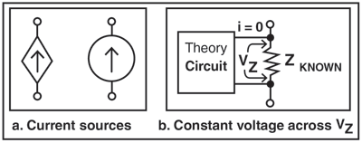
Any good textbook[1] will tell you that a current source supplies constant current and can take on any voltage drop necessary for the source to maintain that current and is drawn like one of the pictures in Fig. 1a . A purely theoretical way to think of what a current source actually does would be what the Theory Circuit would be doing in Fig. 1b . This circuit, if it existed, would control the voltage across a known resistance while maintaining the voltage drop across that component, as shown in Fig. 1b.

Fig. 1: Current-source schematic symbols (a), Constant-voltage current generator (b).
The circuit symbol shown in Fig. 1b would have to work by not doing any work. This circuit would force a voltage across ZKNOWN , without supplying any current to ZKNOWN or drawing any current from the other circuits connected to ZKNOWN . This circuit would always maintain the voltage no matter how fast the load changed; therefore would need infinite bandwidth so it could react rapidly to changing signals and current or voltage surges.
This circuit in the box would force the circuit elements connected to ZKNOWN to supply the current needed to satisfy Ohm’s Law and thus fix the current flowing through ZKNOWN in order to make VZ be the voltage drop.
Although this circuit does not exist, the idea of forcing a known voltage to drop across a known resistance to generate a constant current will be the main theory behind the operation of the current sources discussed throughout this article. The concept of fixing the voltage across a known impedance to generate a known current can be expanded conveniently by use of a programmable resistor to allow in circuit changes to the output current of the circuit.
Design considerations
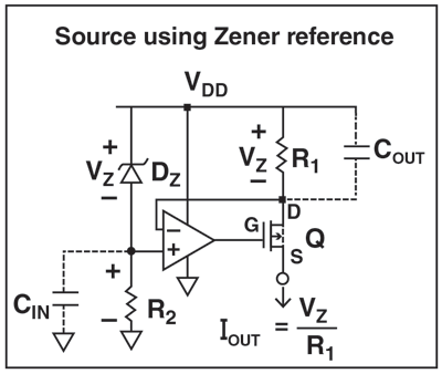
The current source shown in Fig. 2 using the zener diode to generate the reference voltage can be found in The Art of Electronics , by P. Horrowitz and W. Hill.[2] If R1 from Fig. 2 was a programmable resistor then Iout is easily controlled using the I2 C bus or USB. The circuit shown in Fig. 2 is a current source that uses a zener diode to generate a reference voltage, VREF , R1 drops the reference voltage to generate the current, the op-amp and P-Ch channel FET stabilize the loop.
An important key to accuracy is limiting error sources such as noise and offset voltages. This circuit is further improved by use of a few capacitors to aid in noise reduction and for static dc loads. The COUT capacitor has the down side of slowing down the response time of the current source to rapidly changing loads such as transient loads.

Fig. 2: Simple current source using zener diode as voltage reference 1.
When VDD is present the operation of this circuit is defined by the zener diode reverse biasing and dropping the zener voltage (VZ) across its terminals. The current flowing from VDD through the zener diode is limited by R2 . The resistor R2 limits the current to different levels depending on the actual VDD voltage and this component will stabilize the reference voltage generated by the zener voltage.
Another factor that can shift the reference voltage is temperature; therefore it is important to not dissipate a lot of power in the zener so that forces the designer to make R2 have a large ohmic value. Since R2 is generally in the range of 100 kΩ or more, CIN is a valuable addition for diminishing high-speed noise on the non-inverting input by shunting the signal to ground. This will help by keeping the op amp from reacting to undesired high-frequency noise sources.
The pole created by R2 and CIN changes the response of the circuit and increases settling time at start up. Another error source comes from changes in VDD because changes in supply change the current through the zener ,thus making the voltage reference change. This means the current source typically has poor power supply rejection performance.
These errors can be avoided by adjusting R1 or R2 as the power supply is changed. Since the non-inverting input of the op amp is fixed at VDD – VZ , this will be the voltage the op amp will attempt to fix by driving the gate of the P-Ch FET and opening the conduction channel enough to allow the IOUT current to flow.
The addition of COUT will aid in stability by not allowing the voltage to change instantly resistor R1 . The zener should be selected keeping the op-amp input voltage range and output voltage range in mind to prevent the op-amp from saturating into one of the supply rails. It is also beneficial to keep that voltage small so the power in R1 stays low to keep the component from having resistance drift issue caused by heating. The IOUT node can drive any impedance as long as IOUT *load impedance does not exceed VDD VZ .
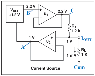
Finally, as the equation in Fig. 2 states, IOUT is calculated simply by dividing VZ by R1 . This is a good current source, but the power supply rejection is poor and loads need to be referenced to ground or special considerations should be made for negative referenced loads. A big improvement can be made through a topology change and the use of an additional op amp and a discrete voltage reference IC. This architecture is displayed in Fig. 3 with a simple low-current example displayed.

Fig. 3: A topology change and the use of an additional op amp and a discrete voltage reference IC.
In the circuit shown in Fig. 3 the dc current will flow from the IOUT node to the Com node. The Com voltage can be any voltage within the power rails of amplifiers U1 and U2 as long as the amplifier stability to operate near their power supply rails are considered. This design uses a LDO as a 1.2-Vdc reference voltage.
The magnitude of the load impedance is limited by the multiplication of IOUT x RL and insuring the IOUT node voltage is less than the positive power rail of U1 minus the reference voltage. Assuming the circuit is operating steady-state, the voltage drop across RL is calculated by multiplying the load impedance by the programmed current (IOUT ).
The IOUT current is found by taking the reference voltage and dividing by the value of resistor R1 . In this example R1 is 1.2 kΩ, so taking the reference voltage divided by R1 , IOUT is found to be 1 mA. Now beginning from the voltage on the Com node and adding IOUT x RL the voltage on the IOUT node is determined. Since U2 is in a buffer configuration, node A is nearly the same voltage as the IOUT node. The LDO takes this voltage and adds 1.2 V to this value which is the voltage at node B. Next, U1 , another buffer forces the voltage on node B to appear on node C. Now node C is fixed and held at the reference voltage above the IOUT node voltage regardless of the value of RL or the voltage on the reference point “Com.” An example has been illustrated with Com held at 0 V and the voltages on each node has been marked assuming the shown component values. In low current applications such as the one shown, U1 may be bypassed to remove the offset error U1 introduces to the system as long as the LDO chosen for the reference has sufficient current delivering capability.
Special considerations
Some special considerations should be made when selecting the components of this circuit. U1 is the main driver amplifier, and therefore should be capable of delivering more current than the highest desired output current setting. The current leaving the IOUT node will always be IOUT = VREF / R1 as a load is present which completes the circuit and neither amplifiers’ input or output are required to rise above the supply rails.
Ideally both amplifiers would operate with rail to rail inputs and outputs voltages to provide maximum current source voltage compliance. It is possible to clamp the output voltage present on IOUT by placing additional zener diodes on node B to ground. This will clamp the voltage on IOUT to the “clamping” zener voltage.
Another way to improve performance is to select high-speed amplifiers, the higher the gain bandwidth product, the faster the circuit will response to changes in the load. As was discussed with the zener referenced current source, noise can be reduced with the addition of a capacitor in parallel with R1 , this capacitor again will not allow the voltage to change instantly across R1 , thus creating a more constant voltage across the resistor that is fixing the current that is output by the source. Some good applications for this type of circuit are loads for devices under test, charging or discharging batteries with the proper use of clamping (can be dangerous to overcharge a Li+ battery), or driving an LED backlight with a constant current.
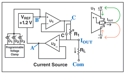
In the spirit of constant improvement and making circuits more ideal and flexible several of the improvement ideas to the source in Figure 3 have been added to the source in Figure 4. Here multiple zener diodes have been added, the idea being each would have a different zener voltage and thus by connecting the cathodes one a time with a programmer, a voltage clamp is created that restricts the IOUT voltage to a safe programmable voltage level by limiting the voltage on node B. Additionally R1 became a programmable resistor allowing for multiple output currents to be achieved via programming or adjusting a potentiometer. A capacitor is also added in parallel with R1 to slow down voltage changes across the resistor and reduce output current noise density. Unfortunately this capacitor reduces the bandwidth and transient response time so care should be taken when selecting the value to obtain the best noise-for-speed trade-off. The final remark is in regard to the source of current for the current source. Regardless of what the load is or what it is tied to, eventually all the current entering the load must return to one of the supply rails powering U1 as shown; therefore the Com node should have the lowest possible impedance path back to the power supply providing power to amplifier U1 .

Fig. 4: Current source improved.
These are all great current sources that should be investigated and used for their simplicity and flexibility. The source in Fig. 4 is especially customizable and the applications are endless, have fun fine-tuning the source to perfectly meet the demands of your load. ■
References-
1. Nilsson, James, and Riedel, Susan. Electric Circuits , Eighth Edition. Prentice Hall. May 2007. Print.
2. Horowitz, Paul, and Hill, Winfield. The Art of Electronics . Cambridge University. July 1989. Print.
Advertisement
Learn more about Integrated Device Technology (IDT)


