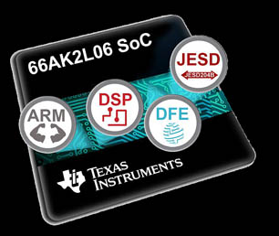
The 66AK2L06XCMS high speed data acquisition SoC uses four 7.37 Gbit/s JESD204B serial link; said to reduce overall board footprints by up to 66% and power by up to 50%. The chips Keystone II architecture has four TMS320C66x 1.2 GHz DSP sub-systems. It also has two 1.2 GHz Cortex-A15 cores with a 1 Mbyte shared L2 memory. The chip features a digital front-end with digital down/up-conversion functionality. The DFE subsystem provides a direct interface to high-speed A/D and D/A converters.

The DSPs each have fixed-point and floating-point capability with 38.4 GMACS/core and 19.2 Gflops/core. Interconnect is via TeraNet non-blocking switch fabrics enabling fast and contention-free internal data movement. The IC has an FFT coprocessor, a five-port Ethernet switch, four GbE ports, a security accelerator, a packet accelerator, USB 3.0, and PCie. It comes in a 900-pin plastic ball grid array and operates over 0° to 100°C or -40° to 100°C. Samples now, production Q3.
Advertisement
Learn more about Texas Instruments


