Data converter ICs deliver
greater efficiency
and smaller size
Power-down modes and design techniques limit
current consumption,
while SOT-23 and µSOIC packages shrink board area
BY LEO McHUGH
Analog Devices
Limerick, Ireland
As key components in many types of port-able equipment, data converter ICs are judged as much on their power consumption and package size as on other performance criteria. Recent trends in these areas indicate just how important these concerns are to designers.

With each new generation of A/D and D/A converters, power requirements are dropping, partly because of advances in component design and partly because of expanded use of power-down functions. Current consumption, which was once rated in terms of milliamperes, is now more commonly specified in microamperes.
At the same time, the use of smaller surface-mount packages is reducing board space requirements. Devices that until recently were offered in 8-pin SOIC packages are now available in SOT-23s and µSOIC packages.
Power-down operation
Powering-down an A/D converter when it is not needed can reduce power consumption, and so power-down is now a standard feature on many A/D converters. Ultimately, powering-down between every conversion results in the largest savings in power, but until recently, the power-up time of the converters has made this impractical.
Several recently introduced A/D converters now offer automatic power-down after every conversion. Analog Devices' parts offer an automatic-power-down mode that is based on the state of the convert-start pin after conversion. This option allows the user to minimize the power consumption at whatever throughput is required. Overall power consumption is therefore directly proportional to the percentage of time the part is at full power compared to the time it is in a power-down state.
Selecting the conversion time to allow for a suitable range of throughputs is the first step in designing the optimum-throughput lowest-power A/D converter. Other parameters that need consideration include power-up time, power-down time, power-down current, power consumption during conversion, and the ability to read the result of a conversion while powered-down.
An example of a power-efficient part is the recently introduced AD7810 from Analog Devices. Operating from a 3-V supply, this 10-bit A/D consumes 6 mW while operating at the maximum throughput of 350 ksamples/s.
However, if a lower throughput is acceptable, the part can be automatically powered-down after each conversion. In power-down, the converter consumes a maximum of 1 µA over the –40° to +105°C temperature range, but this value is typically 200 nA (see Fig. 1 ).
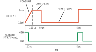
Fig. 1. A/D converters like the AD7810 from Analog Devices can read
the results of a conversion while in the power-down mode, allowing
power consumption to be optimized at whatever throughput is required.
Similar trends can be observed in the D/A converter environment, where current consumption is now specified in microamperes and power-down is a standard feature of most devices (see Fig. 2 ). Among recently introduced devices, the AD5300/ 5310/5320 from Analog Devices are 8-, 10-, and 12-bit D/A converters, respectively, that typically consume less than 120 µA.
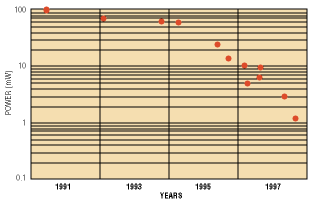
Fig. 2. Over time, D/A converters have improved on power efficiency,
as indicated by the specified maximum ratings for 6 to 12-bit, single-supply,
serial D/As from three manufacturers.
These parts also contain a power-down mode that reduces the current consumption to 50 nA. To reach this low level, new design techniques were necessary. In previous parts, where the power-down current was in the region of 5 µA, a savings of 30 or 40 nA was probably not high on the priority list of the chip's designer.
However, to achieve a power-down current of 50 nA, every nanoampere is important. An example of such attention to detail is turning off the interface logic while it is not in use. This step lowers current consumption by tens of nanoamperes.
Package styles
Although only a few years ago the standard IC package for portable equipment was an 8-pin SOIC package, data converters have since enjoyed significant reductions in package size, as indicated in thetable . Overall size seems to follow power consumption, with each new generation shrinking by an average of 30%.
Package size
| Dimensions (in.) | Package Type (8 leads)• | |||||
| DIP | SOIC | SSOP | TSSOP | µSOIC | SOT-23 | |
| Body length | 0.430 | 0.196 | 0.122 | 0.122 | 0.122 | 0.122 |
| Body width | 0.280 | 0.157 | 0.212 | 0.176 | 0.122 | 0.071 |
| Tip to tip | 0.325 | 0.244 | 0.311 | 0.256 | 0.199 | 0.118 |
| Pitch | 0.1 | 0.05 | 0.025 | 0.025 | 0.025 | 0.037 |
| Height | 0.195 | 0.0688 | 0.078 | 0.039 | 0.043 | 0.057 |
| Total board area | 139.75 | 47.82 | 37.94 | 31.23 | 24.27 | 14.39 |
| (sq mils x 1,000) | ||||||
•SOT-23 has 6 pins.
For A/D converters, the µSOIC package is the smallest package currently available. An example is the previously mentioned AD7810, which comes in an 8-pin µSOIC package.
Meanwhile, D/A converters are being offered in the SOT-23 package, which occupies 40% less board space than the µSOIC package. The aforementioned AD5300/5310/5320 are the world's first 8-, 10-, and 12-bit D/A converters in the SOT-23.
Advertisement


