The engineer must sort out numerous hardware and software perceptions
BY WILLIAM ORME
ARM, Cambridge, U.K.
http://www.arm.com
SoC designs are becoming ever more complex and the level of system integration increasing. Multifunctional, multicore SoCs are now the fastest growing section of ASIC/ASSP IC design starts. Dealing with these complexities with the tradeoff decisions between device costs (silicon area and pin count) and debug and optimization functions can be intimidating (see Fig. 1 ).
Multicore software issues
Many traditional embedded software engineers are concerned about the complexity of writing software for multicore processors. The good news is that most of the complexity can be handled by the operating system. A symmetric multiprocessing (SMP) operating system provides a high-level “threading” API, which makes controlling multiple cores easier.
Most OS vendors have announced or are working on SMP support, which is the easiest way to code for a multicore solution. Linux has good SMP support for many architectures, including ARM MPCore processors, taking full advantage of new processor features such as power-efficient spinlocks (loops), a thread ID register, and memory regions supporting re-ordering memory accesses.
A multicore device often strikes fear into the heart of a programmer who has never targeted such a device. Even for those that have, the experience may have been difficult — with the overhead to support concurrency sometimes greater than the benefit of parallelizing the application. For newer devices, perceptions may need to be changed. These processors have tight integration of the multiprocessing capability, which ensures that the overhead to support concurrency is low and enables very fine levels of software concurrency to realize a performance gain. There is also a well handled implicit concurrency between the active applications, the operating system, and any peripheral drivers. It is really only in situations where a single significant task exists that the programmer may need to consider decomposing this into smaller tasks, just like in traditional single core devices.
Visibility amid rising complexity
To get systems to work well requires visibility into what the system is doing. At some stages, visibility is provided in the modeling tool. However, once you move to a physical implementation, the designer must include mechanisms to provide visibility.
Choosing this mechanism should be a direct response to the needs of different engineers doing all the various project tasks: hardware bring-up, low-level system software, RTOS and OS porting, application development, system integration, performance optimization, production test, field maintenance, and returns failure analysis.
The easy answer is to give full visibility to everything happening on-chip in real time. Most processors offer good debug and trace capabilities, as do multicore interconnect fabrics. On-chip debug and trace, like the ARM CoreSight, can be a critical part of handling many of the issues of multicore. However, these design aids require IP design time or licensing fees, silicon area, IC pins, and design tools, and the engineer needs to decide what is required, beneficial, or only a “nice-to-have.”
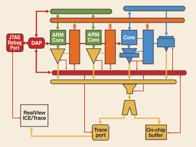
Fig. 1. The implementation of on-chip debug is not a trivial matter.
Run control debug
For multicore SoCs that have cores in multiple clock and power domains, a traditional JTAG daisy-chain should be replaced with a system that can maintain debug communications between the debug tool and the target, despite any individual core being in powered down or sleep mode. The CoreSight Debug Access Port (DAP) is an example of a bridge between the external debug clock and multiple domains for cores in the SoC. This has the secondary advantage of being able to maintain debug communications with any core at the highest frequency supported rather the slowest frequency of all cores, as on a JTAG daisy-chain.
For those requiring ultrafast code download or access to memory-mapped peripheral registers while the core is running, the engineer should connect DMA from the DAP to the system interconnect so that the debug tool can become a bus master on the system bus. For remote debug of in-field products or large batch testing where a debug tool seat per device under test is unrealistic, the designer can also connect the DAP into a processor’s peripheral map allowing the target resident software to set up its own debug and trace configurations.
For multicore systems with interprocess communication or shared memory, the ability to stop and start all cores synchronously is extremely valuable. To ensure this synchronization is within a few cycles, a cross-trigger matrix should be fitted. If, on the other hand, the cores have widely separated and noninterfering tasks, it may be sufficient to synchronize stopping and starting cores with the debug tools, which will inevitably lead to hundreds of cycles of skid between cores stopping.
Sizing a trace subsystem
After run-control debug, real-time trace is the most important debug feature. This is obligatory in hard real-time electromechanical systems where halting the control system is just not an option. Choosing the level of trace has the largest impact on the cost of implementing an on-chip debug system. The good news is that for multicore SoCs the cost per CPU can actually be reduced. The first question to ask is, who is going to use the trace data and with what tool?

Fig. 2. Debug connectivity for asynchronous cores involves cross triggering between cores and intelligent peripherals.
The simplest and cheapest form of trace is that generated by the software executing on the cores themselves. Traditionally this data was written to an area of system memory, while a separate task emptied and sent the data to the debug tools via any available communication channel. The ARM Debug Comms Channel (DCC) over JTAG is an example. Recent optimizations on this approach write to a peripheral such as the CoreSight Instrumentation Trace Macrocell, which streams the trace data directly to a trace buffer (see Fig. 2 ).
For multiprocessing systems, instrumentation trace has the advantage of understanding its own context (for example, which thread am I?). This can add a higher-level semantic that is extremely useful to a software application design engineer. The processor also has access to registers (such as the Performance Monitor Unit of an ARM core) that can provide valuable system performance profiling data. Given the relatively low implementation costs and high potential benefits, instrumentation trace is an obvious candidate to fit in any multicore SoCs.
Where more detail is required or code instrumentation is not adopted, hardware trace, such as ARM Embedded Trace Macrocells, is very popular. Hardware trace — logic that watches the address, data, and control signals within the SoC compress that information and emits it to a trace buffer — can be subdivided into three categories: program/instruction trace; data trace; and bus (or interconnect fabric) trace. Each has different usage models and different costs.
Program trace is highly valuable for both hardware and software debugging and is the main source data required for many profiling tools. The implementation costs of program only trace macrocells can be quite small; thus the bandwidth requirements for a trace port are not too high, even for a 4 x CPU multicore SoC. Where on-chip trace buffers are implemented, a 4-Kbit RAM can hold over 30,000 lines of assembler code execution. That’s a lot of code for an embedded developer to review!
Unfortunately, the cost of implementing data trace is the highest of all. Trace macrocells must be larger, data are more difficult to compress ,and trace buffers must be larger and trace ports faster. The upside is that the needed gates can be squeezed into ever smaller areas, so even high-performance multicore systems can have data trace capabilities if needed.
Multiple on-chip trace buffers can be implemented or trace ports using high speed PHYs can now support multiple Gbit/s lanes. Today’s technology supports up to 6 lanes at 6 Gbit/s, enough for full, cycle-accurate simultaneous program and data trace of three cores running at 600 MHz.
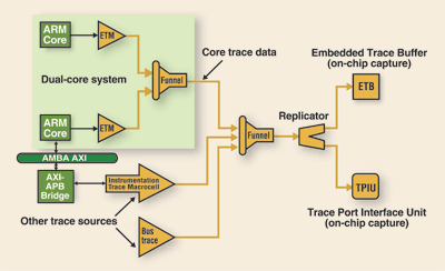
Fig. 3. A trace funnel can combine multiple asynchronous heterogeneous trace streams into one.
Sizing the trace port is another key task for the ASIC designer and another trade-off decision. For multicore SoCs, the best approach may be a combination of solutions. For example, by fitting three parallel trace funnels any subset of trace data may be sent to one of three destinations: a high-bandwidth interface to on-chip trace buffers; a medium-bandwidth trace port to a very deep off-chip buffer; a very narrow (even single-pin) interface for continuous monitoring. This gives a trace solution that can provide for almost any usage case.
Multiple trace sources
As with debug ports, fitting multiple trace ports, one for each core, has obvious silicon and pin overheads. One solution is to use a CoreSight Trace Funnel that combines multiple, asynchronous, heterogeneous trace streams into one. This provides better visibility, a higher bandwidth port or deeper buffer, and substantially reduced implementation overhead when simultaneous trace of multiple cores is required. ■
For more on multicore SOCs, visit http://www2.electronicproducts.com/DigitalICs.aspx.
Advertisement
Learn more about ARM


