By Brian Santo, contributing writer
The Department of Energy is going to spend up to $32 million to fund 16 R&D programs aimed at improving semiconductor power performance. The benefits should be widespread, but the DoE’s key concern is helping to improve data center efficiency.
Data centers suck power like nobody’s business. They already consume 2.5% of the electricity generated in the U.S., and the DoE estimates that figure will double in the next eight years.
The Advanced Research Projects Agency – Energy (ARPA-E) began funding research along these lines in 2013 with a program called SWITCHES, which dealt with advancing bulk gallium nitride (GaN) power semiconductor devices, the manufacture of silicon carbide (SiC) devices using a foundry model, and the design of synthetic diamond-based transistors.
GaN can be more efficient than silicon for power electronics in some circumstances, but silicon has been far cheaper. Silicon is approaching fundamental physical limits in several areas, however.
GaN promises to be the way to go for high-voltage, high-current applications in the future. The material promises lower losses, higher switching frequencies, and higher temperature tolerances. More research is needed to fulfill that promise, however, which prompted the SWITCHES program.
Two follow-ons to SWITCHES were announced in June — one called ENLITENED and the other called PNDIODES.
Participants in the ENLITENED program will be involved in efforts to double data center energy efficiency through new network designs enabled by integrated photonics technologies. They’ll split about $25 million in disbursements.
Participants in the PNDIODES program will divvy up the balance of the total. In general, they’ll be focusing on selective doping in the wide-bandgap (WBG) GaN to create more effective P-N junctions in high-voltage power devices. The WBG GaN and SiC both have bandgaps roughly triple that of silicon (diamond has a bandgap roughly quintuple silicon’s).
Organizations in the ENLITENED program include:
- Ayar Labs, researching co-packaging of optical transceivers with processors
- Columbia University, architectural innovations including connecting processing and memory with unified photonic interconnect; data center “nodes” based on multichip modules (MCM); and new silicon photonics devices
- IBM (1), multi-wavelength, chip-scale optical modules that can be integrated directly with switches or processors; co-packaged optics
- IBM (2), extremely low-power photonic switching devices that operate on the nanosecond scale
- MIT, a unified, light-based communication technology that can be scaled across chip-, board-, and rack-interconnect levels
- UC Berkeley, a new network topology for warehouse-scale computers (WSC)
- UC Santa Barbara, chip packaging with built-in photonic interfaces
- UC San Diego, a new approach combining a unique architecture based on the distributed control of light-based circuit switches; a large-port-count low-loss optical switch technology that routes information carried as light waves; and packaged, scalable, energy-efficient optical interconnect technology designed for the optical switch
- USC will develop a test bed for other technologies in the program. The testbed will create a “virtual internet” that will also allow for testing system security.
Organizations in the PNDIODES program include:
- Adroit Materials, investigating p-type doping using ion implantation of magnesium
- Arizona State University, selective epitaxial growth techniques
- JR2J, laser spike annealing to activate and repair p-type dopants
- Sandia National Laboratories, patterned regrowth of p-n diodes
- SUNY Polytechnic Institute, ion implantation and annealing using a gyrotron beam
- University of Mississippi, neutron transmutation doping
- Yale University, investigating the regrowth process
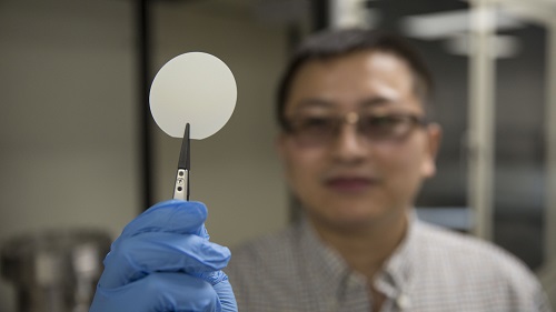
Professor Yuji Zhao (Arizona State University) is working to advance fundamental knowledge of selective area doping processes for gallium nitride wide-bandgap semiconductors. Image: Pete Zrioka/ASU.
ARPA-E will administer the programs. Acting director Eric Rohlfing said, “By accelerating the development of enabling technologies for data center efficiency and advancing innovative fabrication processes for high-performance semiconductors, ARPA-E is furthering its mission to improve the economic and energy security of the United States.”
For the sake of clarity, it is standard practice to provide full names of programs the first time they are used, followed by their acronyms, which are used in subsequent mentions. In this case, the names of the programs involved are brutally long and particularly tortured, apparently so that they can be reduced to acronyms that are vaguely more appropriate than their full names are intelligible.
So for anyone interested, SWITCHES stands for Strategies for Wide-bandgap, Inexpensive Transistors for Controlling High-Efficiency Systems, ENLITENED stands for ENergy-efficient Light-wave Integrated Technology Enabling Networks that Enhance Data centers, and PNDIODES stands for Power Nitride Doping Innovation Offers Devices Enabling SWITCHES, because who doesn’t love a portmanteau acronym? Hope that helped.
Advertisement
Learn more about Electronic Products Magazine


