BY MICHAEL DE ROOIJ,
Executive Director, Applications Engineering,
Efficient Power Conversion,
www.epc-co.com
The popularity of highly resonant wireless power transfer operating at 6.78 MHz has increased dramatically over the last few years, and particularly for applications targeting portable device charging. The surge of interest is driven by the need for convenience and extended battery life. This emerging technology faces many challenges to realize a user friendly product that also complies with the many regulations. Various amplifier topologies, such as the Class E [1, 2, 3], current-mode Class D [4], and voltage-mode Class D [1, 3, 4, and 5] have been presented in the past with varying degrees of success for use in these systems. This article presents a (zero voltage switching) ZVS variation of the voltage mode class D topology, realized using eGaN FETs, demonstrating not only the high efficiency capability, but also the ability to operate over wide load impedance range when driving an Alliance for Wireless Power (A4WP) compliant coil set [6, 7].
eGaN FET’s have previously been demonstrated in various amplifier topologies for wireless power transfer [1, 2, 3, 4, 5, 8, 9, 10, and 11] using a loosely coupled coil set from WiTricity Corporation [12]. eGaN FET based amplifiers consistently achieve higher efficiencies than their MOSFET based counterparts. In this article we again employ eGaN FETs for wireless power transfer, but will now drive A4WP compliant coil sets. The key characteristics of eGaN FET’s that yield higher amplifier efficiency are, their lower gate charge (QG ), zero reverse recovery (QRR ), and higher voltage rating than comparable MOSFET’s. These characteristics also lead to improved performance when the amplifier is operated under non-ideal load conditions typical of the loosely coupled A4WP standard.
The A4WP wireless power transfer standard has emerged as one that addresses the convenience factor for mobile device charging. To accommodate a wide variety of real-life consumer situations, the specifications require design for a large variation in coil impedance due to variations arising from changes in load conditions. An amplifier driving these coils needs to either be capable of driving such large impedance variations or utilize some form of adaptive matching. In the case of a class 3 coil (targeting small tablet applications), the amplifier needs to be capable of driving a real reflected impedance (as seen by the amplifier) range from 0 Ω through 55 Ω. In this article, the imaginary component variation will be ignored as this can be dealt with using adaptive matching circuits, and the variation induced by dc load resistance change is very small. For a class 3 coil the power limit is 16 W and it needs to support up to two category 3 device coils. For class 4 (targeting higher power tablets) the power limit is 22 W and it needs to support up to three category 3 device coils. The category 3 device coil power limit is 6.5 W and is based on a single smart phone charging requirement.
ZVS Class D vs Class E
The ZVS Class D topology is shown in Fig. 1 (left) together with the ideal operating waveforms. The entire coil circuit that includes the source coil, device coil, device matching and rectifier can be simplified into an equivalent impedance Zload [3, 4, 5, and 11]. The ZVS tank circuit is used to establish ZVS transitions for the switching devices without the use of the highly resonant circuit as implemented in the class E topology, shown in Fig. 1 (on the right).
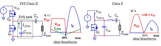
Fig. 1: (left) ZVS Class D topology with ideal waveforms, (right) Class E topology with ideal waveforms.
The design of the ZVS tank circuit capacitance value is simply chosen to have a low ripple voltage, and the inductance is dependent on the supply voltage (VDD ), device COSS , and required transition time under ZVS conditions.
The design of the class E amplifier is more complex as it requires a choice of Q-factor for the circuit in addition to the supply voltage (VDD ), device COSS , and load impedance (Zload ). The intimate inclusion of Zload into the design process indicates that optimal operation of the class E amplifier becomes very sensitive to load variations [3, 5].
Experimental verification
The performance of an eGaN FET based ZVS class D, and a MOSFET based class E amplifier were tested using the same Class 3 source and a single category 3 device coil [7]. Output power was pushed beyond that specified in the A4WP standard [7] to demonstrate the capability of both amplifiers. Both coils were tuned without the presence of metal objects or magnetic materials. The device board includes a rectifier with output filtering and was placed 5 mm above the source coil with both winding centers aligned. Both amplifiers are designed to operate with the same coil set and load specifications.
The peak performance efficiency (based on the specific load condition that yields the highest efficiency) comparison between the ZVS class D and Class E amplifiers driving the A4WP coil set is shown in Fig. 2 (left). Highlighted on the graph are the power ranges for a single category 3 device, two category 3 devices, Class 3 power limit, and class 4 power limit. It can be seen that the ZVS Class D, fitted with the EPC8009 eGaN FET, can operate well above the prescribed power limits of the A4WP standard with efficiencies over 10 percentage points higher than the MOSFET based Class E. Also shown on the graph is the amplifier supply voltage for each of the amplifiers. The experimental circuits used during testing are shown in Fig. 2 (right). Operation using differential mode versions of the amplifiers will halve the supply voltage needed to operate at the same power level for both topologies.
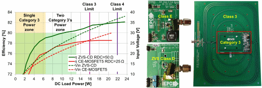
Fig. 2: (left) Peak performance efficiency and supply voltage comparison between the ZVS class D and Class E amplifiers, (right) Photos of the experimental amplifiers and coils.
The load regulation (Vout set to 15 Vdc by varying the input voltage) performance efficiency comparison between the ZVS Class D and Class E amplifiers is shown in Fig. 3 (left). Highlighted on the graph are the power ranges for a single category 3 device, two category 3 devices, Class 3 power limit and Class 4 power limit. The graph clearly shows the superior performance of the ZVS Class D amplifier compared to the Class E over a wide load range. Only below 25 Ω dc load resistance does the Class E show slightly higher efficiency over the ZVS Class D, which is a strong function of coil tuning. In the case of the Class E, the source coil is designed to operate more efficiently at 25 Ω dc load resistance whereas the ZVS Class D is designed to operate at peak efficiency at 50 Ω. This is due to the design criteria, where in the case of a Class E topology, designing to 50 Ω yields extremely high device losses when operated with low dc-load resistance. The ZVS Class D design yields a more even distribution of losses over the dc-load variation range.
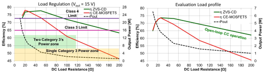
Fig. 3: Load regulation efficiency comparison (left) and single Category 3 load variation efficiency comparison (right) between the ZVS Class D and Class E amplifiers .
Since mobile device charging will be a primary function for wireless power technologies, a single category 3 was operated with a load that would emulate a charging battery and is shown in Fig. 3 (right). Again, it can be seen that the ZVS Class D efficiency is higher than the Class E over nearly the entire range with only a small range being equal. Also shown on the graph is the load power where the peak is set to the category 3 limit of 6.5 W.
The peak performance thermal comparison between the two amplifiers is shown in Fig. 4 . It can be observed that the ZVS Class D amplifier’s peak temperature is nearly 10°C cooler than the Class E amplifier under similar load power conditions. Both amplifiers were operating with no heat-sink present and no forced air cooling in an ambient of 25°C. It is further notable that the hottest component on the ZVS Class D amplifier is the gate driver whereas it is the MOSFET in the Class E amplifier.
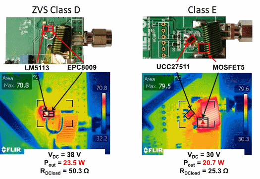
Fig. 4: Peak power thermal comparison between the ZVS Class D (left) and Class E (right) amplifiers .
eGaN FETs continue to be a disruptive and enabling technology and in this article the advantages of GaN in 6.78 MHz highly resonant loosely coupled wireless power transfer was shown. An eGaN FET based ZVS class D amplifier operates more efficiently than a MOSFET based class E amplifier under large load variations, achieving efficiencies over 10 percentage points higher.
References
[1] A. Lidow, J. Strydom, M. de Rooij, D. Reusch, “GaN Transistors for Efficient Power Conversion,” Second Edition, Wiley, ISBN 978-1-118-84476-2
[2] W. Chen, et al., “A 25.6 W 13.56 MHz Wireless Power Transfer System with a 94% Efficiency GaN Class-E Power Amplifier,” IEEE MTT-S International Microwave Symposium Digest (MTT), pg. 1 – 3, June 2012.
[3] M. A. de Rooij, “Performance Evaluation of eGaN FETs in Low Power High Frequency Class E Wireless Energy Converter,” International Exhibition and Conference for Power Electronics, Intelligent Motion, Renewable Energy and Energy Management (PCIM – Asia), June 2014, pg 19 – 26.
[4] M. A. de Rooij, “eGaN FET based Wireless Energy Transfer Topology Performance Comparisons”, International Exhibition and Conference for Power Electronics, Intelligent Motion, Renewable Energy and Energy Management (PCIM – Europe), May 2014, pg. 610 – 617.
[5] A. Lidow, M. A. de Rooij, “Performance Evaluation of Enhancement-Mode GaN transistors in Class-D and Class-E Wireless Power Transfer Systems”, Bodo Magazine, May 2014, pg. 56 – 60.
[6] R. Tseng, B. von Novak, S. Shevde and K. A. Grajski, “Introduction to the Alliance for Wireless Power Loosely-Coupled Wireless Power Transfer System Specification Version 1.0,” IEEE Wireless Power Transfer Conference 2013, Technologies, Systems and Applications, May 15-16, 2013.
[7] “A4WP Wireless Power Transfer System Baseline System Specification (BSS)” Ver. 1.1.2+ October 07November 14, 2013.
[8] M. A. de Rooij, J. T. Strydom, “eGaN FET- Silicon Shoot-Out Vol. 9: Wireless Power Converters,” Power Electronics Technology, July 2012, pg. 22 – 27.
[9] M. A. De Rooij and J. T. Strydom, “eGaN FETs in Low Power Wireless Energy Converters,” Electro-Chemical Society transactions on GaN Power Transistors and Converters, Vol. 50, No. 3, pg. 377 – 388, October 2012.
[10] A. Lidow, “How to GaN: eGaNFETs for High Frequency Wireless Power Transfer,” EEWeb: Power Developer Magazine, pp. 4 – 9, January 2013.
[11] A. Lidow, “How to GaN: Stable and Efficient ZVS Class D Wireless Energy Transfer at 6.78 MHz,” EEWeb: Pulse Magazine, Issue 126, pp. 24 – 31, July 2014.
[12] Witricty Corp. coil set part numbers 190-000037-01 and 190-000038-01, www.witricity.com
Advertisement
Learn more about Efficient Power Conversion (EPC)


