Digital power improves power-supply efficiency
The green concept is behind the push to improve
power supply efficiency at light loads – now to do it
BY ALEX DUMAIS
Microchip Technology, Chandler, AZ
http://www.microchip.com
Many applications today, such as internal power supplies for PCs, may operate in light-load conditions (
With the recent push for “green energy,” power-supply designers have been challenged to improve the efficiency of their power supplies. One challenge has been to improve the efficiency at low-load conditions while still maintaining high efficiency at large loads.
Power-supply losses
To improve efficiency in switch-mode-power-supply (SMPS) applications, we first need to understand the fundamental losses within a power-supply application. For this example, we will look at a step-down converter (buck converter); more specifically, a synchronous buck converter design (see Fig. 1 ).
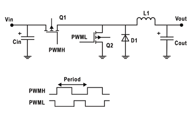
Fig. 1. Synchronous buck converter.
In synchronous buck converter applications, the majority of the losses in the system occur in the MOSFET conduction and switching losses. SMPS applications with high switching frequencies will endure higher switching losses, as the switching losses increase with switching frequency.
At large loads, conduction losses will contribute a larger percentage of the total power loss. Conduction losses can be minimized by selecting proper MOSFETs with a low drain-to-source resistance (RDS(on) ). MOSFET power losses can be approximated by the following equations:
P(MOSFET_CONDUCTION) = Irms 2 RDS(on)
P(MOSFET_SWITCHING) = 0.5 Vin Fsw Ipeak (Tr + Tf )
Within the context of this article, the inductor and capacitor power losses are minimal in comparison to the MOSFET losses. This can be accomplished by selecting proper components with low ac/dc resistance characteristics. The following equations provide the losses seen from the inductor and capacitor:
P(INDUCTOR) = Iout 2 DCR + Core loss (f(fsw))
P(CAPACITOR) = Iripple_rms 2 ESR
In light-load conditions, the inductor, capacitor and MOSFET (conduction) losses are negligible, leaving the MOSFET switching losses as the main source for power loss.
From the MOSFET switching equation, it can be seen that switching losses in the system can be reduced by reducing the switching frequency or by selecting a MOSFET with faster gate rise and fall times. In both cases, this is not ideal because reducing the switching frequency can result in poorer transient response and may result in a higher-output ripple voltage. Selecting MOSFETs with faster gate rise and fall times could result in an increase in switching noise, as well as the need for stronger gate drivers to drive the MOSFETs.
So, how else can synchronous buck converter applications become more efficient at light loads?
Improving efficiency
Multiphase synchronous buck converters are often used to increase the power handling of a step-down voltage stage. Multiple converters in parallel increase performance while reducing the output ripple current and allowing the use of smaller components. However, at light loads, having multiple converters switching may decrease the efficiency of the system.
When operating at low current , it may not be necessary to have all converters operating simultaneously. Depending on the load current, multiple converters can be disabled, eliminating MOSFET switching and conduction losses for each stage. As the output-load current increases, individual converter stages can be enabled to handle the output-load current.
The idea is to measure the output-load current and compare it to a threshold value, which will determine when to disable/enable individual buck-converter stages. At this point, the PWM drive signals will need to be asserted/deasserted, depending on the load current.
A similar technique can be applied to a single-phase buck converter. The synchronous-buck MOSFET Q2 can be disabled/enabled when the measured output current crosses a threshold. As the load current is light, by disabling MOSFET Q2, conduction and switching losses will be eliminated while dynamic response and output voltage will not be affected. This technique works in the range from no-load conditions to the maximum current ratings of the synchronous diode D1.
In both cases, having full control of the PWM drive signals is essential. The PWM module should allow some PWM drive signals to remain active while other drive signals are in an override state (disabled).
Figure 2 demonstrates the power savings as a percentage gained when implementing these techniques. The top graph shows the results of the synchronous buck converter testing. The converter tested was designed for 23 A at 3.3 V. The bottom graph shows the results of testing a multiphase synchronous buck application designed for 69 A at 3.3 V.
fapo_Microchip02_aug2009 Fig. 2. Results of the MOSFET enabling/disabling technique.
At 10% load, the measured efficiency of the power supply was 54%. By disabling MOSFET Q2 when the synchronous buck converter is operating in low-current conditions, the measured efficiency was 65%. The result is a 20% increase in efficiency.
As for the multiphase converter, at 10% load, the measured efficiency was 61%. By disabling multiple converters when in low-current conditions, the measured efficiency was 75%. This is a 23% increase in efficiency at 10% load.
Executing these techniques may not be straightforward with a purely analog approach. However, a digital controller can easily implement these techniques with its knowledge of the changing load conditions, without the need for additional circuitry. The following section looks at the advantages of digital controllers via their built-in peripherals.
Digital considerations
Digital signal controllers (DSC) can ease the process of improving the efficiency of dc/dc point-of-loads, due to their on-chip peripherals and software capabilities. DSCs with specialized power-conversion peripherals, such as the dsPIC33 GS series, enable greater power-supply efficiencies via fully digital control loops.
When selecting a DSC, it is important to have a high-resolution PWM module with flexible PWM output control. The ability to override (disable) individual PWM channels on the fly will allow simple implementation of the techniques discussed in this article.
The override feature is useful in many types of applications. For instance, in an offline uninterruptible power supply (UPS), when the ac line is present, the PWM module is used to charge the batteries and possibly to drive internal dc fans. During this time, the PWM drive signals for the inverter will remain in an override state. If a failure occurs on the ac line, the inverter override signals are removed and the PWM drive signals for the battery charger are placed in their override state.
Additionally, look for DSCs that offer on-chip analog comparators and high-speed ADCs. Analog comparators can reduce the processor workload, leaving more time to process ADC samples and monitor current/voltage feedback signals.
An integrated ADC module with independent sample-and-hold circuits allows the DSC to sample voltage/current feedback signals at a precise moment within the PWM cycle. Analog comparators as well as PWM and ADC modules are the most important peripherals to consider when designing switch-mode power supplies.
The availability of reference designs, code examples, and software libraries make designing power supplies with DSCs easier than ever. Designing supplies with DSCs can improve system efficiency at low loads, while maintaining high efficiency at full load — reducing component count, cost, and development time. ■
Advertisement
Learn more about Microchip Technology


