By Gina Roos, editor-in-chief
Medical devices encompass a range of products, from ultrasound equipment and implantable devices to home blood glucose meters and fitness trackers. Each application calls for different requirements, but they are all looking for microprocessors (MPUs) and microcontrollers (MCUs) that can deliver performance in the areas of execution, reliability, security, power savings, and connectivity. Many of these same performance enhancements can be used across a variety of applications.
The increasing adoption of wearable electronics and the need for medical electronics that track and monitor a patient’s health are being driven by an aging population and growing health awareness. The explosion in connected medical devices also is driving chipmakers to address cybersecurity risks at the chip level.
Ultra-low-power consumption is particularly important in applications that need to access real-time signals, such as temperature, acceleration, and speed. One trend noted in a MarketsandMarkets report is the need for ultra-low-power microcontrollers with analog peripherals. Benefits include high reliability, reduced noise, low latency, and decreased costs, which can be advantageous in medical or health-care devices, such as blood glucose meters, heart rate monitors, and implantable devices.
An example of a low-power microcontroller with integrated programmable analog is the Synergy S1 MCU series from Renesas Electronics Corp. Designed to simplify design and reduce bill of materials (BOM), the S1JA MCU Group features a 48-MHz Arm Cortex-M23 core and programmable analog and security functions for high-accuracy sensor signal acquisition and conditioning. These MCUs can be used in a range of cost-sensitive and low-power industrial internet of things (IIoT) sensor applications. These include headline medical monitors, flow control meters, multi-sensor systems, instrumentation systems, and single-phase electricity meters.
The S1JA Group includes five MCUs with 256-KB flash memory, 32-KB SRAM memory, and a wide operating voltage range of 1.6 V to 5.5 V. Each MCU integrates a sensor-biasing unit that supplies accurate power to the external sensor, and a highly configurable analog fabric that processes complex algorithms to maximize signal conditioning and precise analog measurements, said Renesas.
The S1JA MCUs enable advanced analog configurations, from basic functions to more complex analog blocks, enabling designers to eliminate several external analog components. On-chip analog components include a high-accuracy 16-bit analog-to-digital converter (ADC), 24-bit sigma-delta ADC, fast-response 12-bit digital-to-analog converter (DAC), rail-to-rail low-offset operational amplifiers, and high-speed/low-power comparators.
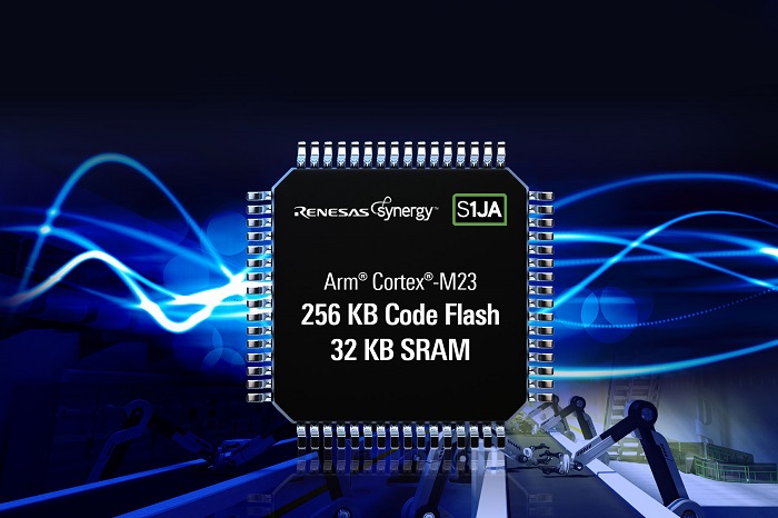
Renesas’ S1JA MCUs enable advanced analog configurations, from basic functions to more complex analog blocks. (Image: Renesas Electronics)
The microcontrollers’ ultra-low power extends battery life for battery-operated portable and battery backup applications. The software standby mode consumes only 500 nA to enable 20-year battery-operated applications that spend extended periods in sleep mode.
In addition, the microcontrollers are packed with security features, including an integrated AES cryptography accelerator and true random number generator (TRNG), and memory protection units provide the fundamental blocks to develop a secure system that connects to the cloud.
The Renesas Synergy Software Package (SSP) supports the S1JA MCUs with HAL drivers, application frameworks, and RTOS. The SSP also includes six modules that simplify interconnecting the configurable internal analog blocks. Embedded-system designers can use either of the Renesas Synergy development environments — e² studio or IAR Embedded Workbench — to build and customize their designs.
Renesas also developed a reference design/solution that can be used for wearable galvanic skin response products and handheld body composition meter systems. Galvanic skin resistance (GSR) and body composition monitor (BCM) measurements provide biometric information that can be used in inferring emotional state and calculating body fat mass, respectively.
This battery-powered device takes DC conductance measurements in GSR mode and high-precision AC impedance measurements in BCM mode while consuming low power. The resolution and speed of the ADCs are critical to the accuracy of GSR-BCM measurements, along with skin temperature compensation, said Renesas.
The GSR-BCM solution leverages the Synergy S1JA MCU for its analog and low-power features. It also includes the Renesas RL78/G1D for Bluetooth connectivity and the ISL9203A for Li-ion battery charging.
The RL78/G1D is a 16-bit MCU with Bluetooth low-energy support and low-current consumption at 4.3 mA RF transmission current (0 dBm output) and 3.5 mA RF receiving current. The circuit elements needed for antenna connection are built in, which simplifies circuit design and lowers the cost by eliminating the need for external parts. The software stack supports wireless software updates.
The ISL9203A is an integrated single-cell Li-ion or Li-polymer battery charger capable of operating with an input voltage as low as 2.4 V. It works with various types of AC adapters.
For portable and wireless designs, such as fitness trackers, these applications require low-power consumption, enhanced security, and multi-protocol support.
A recent example is Samsung Electronics’ Exynos i T100 , which integrates a processor and memory in a single chip and supports Bluetooth 5 Low Energy, Zigbee 3.0, and Thread protocols. For enhanced wireless connectivity functionality, the chip offers a multi-radio concurrent mode that supports two different protocols simultaneously. So, it can support Bluetooth and Zigbee or Bluetooth and Thread at the same time.
Designed to enhance the security and reliability of devices for short-range communications, such as fitness wearables, smart lighting, and home security and monitoring, the chip offers security features that protect against potential hacking and other threats. The solution provides a separate security subsystem (SSS) hardware block for data encryption and a physical unclonable function (PUF) that creates a unique identity for each chipset.
The Exynos i T100 consists of an Arm Cortex-M4F that runs at up to 100-MHz clock speed and high-density memory including 1.2-MB flash memory and SRAM that provides 192 KB and 24 KB. In addition, it can operate in extreme temperatures as low as -40°C and up to 125°C.
Samsung also offers a reference solution for faster development. The reference board supports the Shields interface that can be plugged on top of an Arduino board for testing and controlling sensors. It also provides operating system and embedded APIs for connectivity protocols for developing custom applications.
Designed for high-performance health and wellness, smart home, industrial, and consumer applications, STMicroelectronics’ STM32MP1 multi-core microprocessor series with Linux distribution extends the STM32 microcontroller portfolio with enhanced performance, resources, and open-source software. The STM32MP1 with compute and graphics support offers power-efficient, real-time control and high feature integration.
The STM32MP1 series enables designers to develop a new range of applications using the STM32 heterogeneous architecture that combines Arm Cortex-A and Cortex-M cores. This architecture delivers fast processing and real-time tasks on a single chip, while providing high power efficiency.
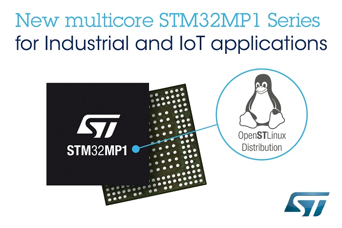
STMicroelectronics’ STM32MP1 delivers enhanced performance, resources, and open-source software. (Image: STMicroelectronics)
ST cites examples of its power savings. By stopping Cortex-A7 execution and running only from the more efficient Cortex-M4, power can typically be reduced by 25%. Shifting from this mode to standby further cuts power by 2.5 k times while supporting the resumption of Linux execution in 1 to 3 seconds, depending on the application.
The STM32MP1 embeds a 3D graphics processor unit (GPU) for human-machine interface (HMI) displays. It supports a range of external DDR SDRAM and flash memories. It also embeds a large set of peripherals that can be allocated to either Cortex-A/Linux or Cortex-M/real-time activities. The STM32MP1 series is available in a range of BGA packages.
ST offers two evaluation boards ( STM32MP157A-EV1 and STM32MP157C-EV1) and two Discovery kits (STM32MP157A-DK1 and STM32MP157C-DK2).
In addition, three developer packages are available, depending on a designer’s needs:
- Starter Package (STM32MP1Starter) to quickly start with any STM32MP1 microprocessor device
- Developer Package (STM32MP1Dev) to add one’s own development on top of the STM32MP1 embedded software distribution
- Distribution Package (STM32MP1Distrib) to create one’s own Linux distribution starter or developer packages
Big data
Moving and analyzing massive amounts of data is a big challenge across numerous end markets. These segments include medical imaging, medical devices, wireless consumer electronics, and factory and building automation. Sharing more data requires higher security, better interoperability, faster processing, and consistent and higher-quality communications.
Texas Instruments Inc. (TI) introduced two devices earlier this year using its bulk acoustic wave (BAW) technology designed for use in applications with high data transmission, such as connected medical equipment. These new devices are the SimpleLink CC2652RB wireless MCU and the LMK05318 network synchronizer clock for high-performance data delivery.
The BAW technology integrates reference clocking resonators to provide the highest frequency in a small footprint, which improves performance and increases resistance to mechanical stresses, such as vibration and shock. This results in stable and continuous data transmission, delivering more precise data synchronization of wired and wireless signals, so data can be processed quickly for higher efficiency.
Incorporating a complete RF system and an on-chip DC/DC converter, the CC2652RB is touted as the industry’s first crystal-less wireless MCU. It integrates a BAW resonator in the QFN package and eliminating the need for an external high-speed 48-MHz crystal. The higher integration also delivers a 10% to 15% savings in printed-circuit-board (PCB) space.
The CC2652RB device provides excellent battery life and allows operation on small coin-cell batteries and in energy-harvesting applications thanks to its very low active RF and MCU current, in addition to sub-µA sleep current with up to 80 KB of parity-protected RAM retention.
The CC2652RB device combines a very low-power RF transceiver with a 48-MHz Arm Cortex-M4F CPU in a platform supporting multiple physical layers and RF standards. A dedicated radio controller (Arm Cortex-M0) handles low-level RF protocol commands that are stored in ROM or RAM for ultra-low power and greater flexibility. The sensor controller, with its fast wakeup and ultra-low-power 2-MHz mode, is designed for sampling, buffering, and processing both analog and digital sensor data, said TI, which maximizes sleep time and reduces active power in the MCU system.
In addition, the chip claims to be the lowest-power, multi-standard device supporting Zigbee, Thread, Bluetooth Low Energy, and proprietary 2.4-GHz connectivity solutions on a single chip. It operates over a -40°C to 85°C temperature range, unlike many crystal-based solutions currently on the market. A CC2652B SimpleLink MCU-based TI LaunchPad development kit is available.
Chipmakers such as Intel Corp. also see artificial intelligence (AI) moving into medical imaging applications and other areas, including acute- and critical-care and diagnosis, which require a lot of processing power. At one time, the only real hardware solutions for deep learning were GPUs.
Today, Intel offers the Xeon Scalable processors (introduced in 2017), which can handle complex hybrid workloads, including memory-intensive models typically found in medical imaging.
Intel worked with Philips to show that servers using Intel’s Xeon Scalable processors can perform deep-learning inference for x-rays and computed tomography (CT) scans without the need for hardware accelerators. The tests show that for many AI workloads the Xeon Scalable processors performed better than GPU-based systems.
The companies tested two healthcare imaging proof of concepts : one on x-rays of bones for bone-age-prediction modeling and the other on CT scans of lungs for lung segmentation. Using the Intel Distribution of OpenVINO toolkit and other software optimizations , Philips was able to improve speed by 188x in images per second for the bone-age-prediction model and 37x for the lung-segmentation model over the baseline measurements.
Advertisement
Learn more about Electronic Products MagazineRenesas Electronics AmericaTexas Instruments


