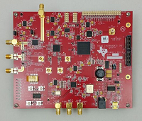
The I/Q Correction block implemented in the Field Programmable Gate Array (FPGA) of the TSW6011EVM helps users to adopt a direct down conversion receiver architecture in a wireless system. The I/Q correction block consists of a single-tap blind algorithm, which corrects the frequency-independent I/Q imbalance in a complex zero-IF receiver system. Along with the I/Q correction block, the FPGA includes a digital gain block, a digital power-measurement block, x2 of interpolation block, an I/Q offset correction block, and a quadrature mixing block.
Features:
Direct Down conversion receiver signal chain with automatic IQ correction
Includes TRF371125 IQ demod for direct conversion to baseband
ADS5282 to capture the IQ receive signal for IQ processing
Automatic blind IQ correction IP example provided on Altera Cyclone III FPGA
Parts Include:
ADS5282 Low Power 8-Channel, 12-Bit, 65MSPS ADC with Serialized LVDS Interface
CDCE62005 5/10 Outputs Clock Generator/Jitter Cleaner with Integrated Dual VCO
DAC5672 14 bit 275 MSPS Dual Digital to Analog Converter
Learn more by downloading the reference design below
Advertisement
Learn more about Texas Instruments


