Moore’s Law is an observation made by Intel founder Gordon Moore that the number of transistors on an IC doubles approximately each 24 months, and the distance between transistors is inversely proportional to the processing speed of a computer. The law, in place for decades, therefore implies that the speed of processors due to transistor density doubles each 24 months. By factoring in improvements due to individual transistor speeds, however, the growth rate of net processor performance actually doubles each 18 months.
Can Moore’s Law continue? That will depend on the industry tackling such issues as the dramatic increase in costs, and the fact that the internal heat of the processor rises as transistor density increases, resulting in both overheating and excessive energy requirements. Challenges based on physics also exist, where limitations involve the speed of light, quantum scale, and gravitational and Boltzmann constants.
While processing in the future will likely involve quantum processors that use particle interactions on a quantum scale and harness the fact that photons and atoms can exist in multiple states, storing information and perform processes, Moore’s Law should be in place for quite some time.
The majority of ICs are built using planar transistors where the silicon channels that conduct electron flow when the switch is on or off, lie flat on a silicon base. Until 2005 it was possible to shrink the features on these planar transistors and maintain performance and reliability. At 90 nm, however, gates that control the switching of transistors began to leak resulting in a power problem.
Intel realized that major changes to the design of transistors to combat heat and power efficiency issues would be necessary if Moore’s Law were to continue. Two changes in particular were involved. First, swapping out standard silicon dioxide insulators in transistors in favor of efficient high-k metal-gate (HKMG) insulators took place when Intel went to the 45-nm manufacturing process allowed for thicker insulating layers to control gate leakage without sacrificing performance. The second, and most important change was the introduction of Tri-Gate or 3D transistor technology.
Enter Tri-Gate
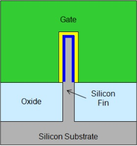
A 3D or nonplanar transistor structure is referred to as a field-effect transistor (FinFET), since the conducting channel sticks up from the substrate like a fin with a gate on either side to improve switching control. FinFETs have a relatively thin and tall fin, which is difficult to manufacture. Intel’s Tri-Gate design, in comparison, surrounds the channel on three sides so that it can effectively control a shorter, wider, and easier-to-build fin. This reduces the sub threshold leakage current form source to drain in the “off” state. The power supply voltage is reduced and superior speed maintained because of the increased effective width, contributing to substantial power savings.

Fig. 1: Intel schematic drawing of a Tri-Gate transistor.
Tri-Gate transistors third gate over the channel. The design reduces leakage and lowers power needs. At 22 nm, for example, Tri-Gate transistors deliver 37% better performance than the 32nm planar transistors used in Sandy Bridge chips. The key performance advantage of Tri-Gate geometries is in the effective width of the conducting channel. The current drive capability and performance of a transistor is directly proportional to its effective channel width, which can be enhanced in 3D structures as the width is extended in the third dimension without layout impact.

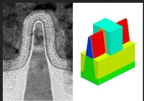
Fig. 2: Intel’s FinFET triangular shape.
The International Technology Roadmap for Semiconductors (ITRS) has identified this 3D Tri-Gate transistor technology as a primary enabler of all incremental semiconductor improvements beyond the 20- or 22-nm design node.

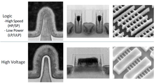
Fig. 3: TEM linear- and cross-sections of, and tilted SEM of logic (top) and high-voltage (bottom) transistors. (Source: Intel.)
Beyond 14 nm, several technologies are being researched to take Moore’s Law all the way to 10, 7, and 5 nm. Those under study include 111-V and 3D transistors, grapheme, EUV lithography, dense memory, materials synthesis, thinner interconnects, photonics, and nanowires.
As processes continue to migrate downwards, challenges increase. They include:
• Converting to double patterning for tighter pitches using an extra step in the lithography process
• Creating interconnects in a chip already extremely dense with transistors that when using skinnier wires, reliability and performance suffer.
At the 10-nm level, the main challenge will be current leakage, and solving it depends on breaking through the 10-nm physical gate length barrier. A huge obstacle to shrinking faster processors is the lack of a proper light source.
Today, etching involves a deep ultraviolet wavelength of 193 nm. At 28 nm, limits were reached at what the wavelength could etch. Enter Extreme ultraviolet lithography, which is schedule to be ready by 2015 as long as two challenges can be solved: strength of the light source and exposure time.
Generating EUV at the intensities necessary for mass production requires up to an order of magnitude more input power than currently available with conventional lithography. A higher-power system can etch wafers faster, but the power requirements can go into the kilowatt range for each piece of equipment. It is estimated that EUV requires 1,000 W of source power to hit its production targets.
FPGAs and Tri-Gate
Recently announced, Altera Corporation is moving production of its Stratix family of FPGAs to Intel’s 14-nm Tri-Gate process technology, enabling its customers to design the most advanced highest performing FPGAs in the industry. ]
Control over static and active power dissipation improves tremendously with Tri-Gate. For FPGA users this makes programmable logic that advances to 1-nm technology and beyond power competitive with ASIC and ASSP design solutions.
Users of Altera’s high-density and high-performance FPGAs on 14 nm process will experience dramatic performance in FPGAs including a historic doubling of core performance compared with other FPGAs, bringing on gigahertz performance levels. Overall, active and static power numbers will reduce by 70% through process, architecture and software advances.
Today, Altera has more than 50% of the high-end FPGA market. At 14 nm, it will have the only product line capable of competing in the high-end of the FPGA market for the next several years. And, its customers do not have to wait until the 14-nm product hits the shelf. Users can begin designs using Altera’s Arria 10 portfolio of 20-nm FPGAs, taking advantage of pin-for-pin design migration from Arria to Stratix 10 FPGA and SoC products as soon as they are available.
Delivering Intel and Altera worldwide
Mouser customers are in a prime position to take advantage of process-technology developments at both Intel and Altera. With worldwide distribution agreements in place with both companies, customers will have direct access to Intel’s entire portfolio of mobile, desktop, and server products. Included in Mouser’s Intel portfolio are the latest 22 nm Core i7, i5, i3, Pentium, Celeron, and Xeon processors – ranging from the most advanced 4th Generation Core through previous Generation Core and Atom processors. Also available are Express Chipsets, Ethernet controllers, system controllers, and Intel’s Next Unit of Computing (NUC).
Mouser’s distribution agreement with Altera includes Altera’s full range of products. Mouser’s Web site will also provide design engineers easy online access to Altera technical documentation for ease-of-design and increased productivity.
As Intel and Altera continue to bring new capabilities to the industry, Mouser’s will continue ensure that its customers are in the best position possible to take advantage through training, design assistance, access, and real-time product information.
Advertisement
Learn more about Mouser Electronics


