BY PATRICK MANNION,
Contributing Editor
The do-it-yourself (DIY) maker movement continues to grow, encouraging hardware and software vendors to leapfrog each other in terms of higher performance at lower cost. They are also competing aggressively for community participation to add more software and enlarge their critical ecosystems of support and, in return, are providing enhancements to their core offerings, including wireless connectivity for IoT projects.
The interest in DIY and its associated embedded prototyping and development space has also prompted other major companies to enter the arena with varying degrees of success. For example, Intel tried its hand with the Atom-based Joule Compute Module in late 2016 but pulled the plug in mid-2017. Meanwhile, Samsung is finding success with its Exynos heterogeneous multicore processors via Hardkernel’s Odroid offerings. Other communities have experienced a surge in popularity, such as BeagleBoard.org Foundation.
As the offerings multiply, hobbyists and professionals alike need to choose according to the requirements of the application. These requirements include I/O, processing horsepower, memory, cost, ecosystem support, and the likelihood of a design going into full production. Also, as wireless plays a larger role, hobbyists and developers alike need to be aware of regulations around RF emissions if they intend to sell their projects or designs. Distributors will disable wireless if it’s not certified.
Arduino, Raspberry Pi, and BeagleBone still rule
While many are entering the space, DIY and prototyping boards are dominated by the Arduino, Raspberry Pi, and BeagleBone platforms. Both Arduino and Raspberry Pi started as learning tools for kids and hobbyists: Both communities still reflect their origins. The BeagleBone requires some more programming knowledge, and it’s the most suited to being deployed as a full-on embedded system.
Of the three, the Raspberry Pi (R-Pi) is arguably the most recognizable and widely DIY SBC. The Raspberry Pi 3 Model B is the latest revision of their flagship line and has impressive hardware for a little board (Fig. 1 ).
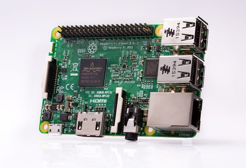
Fig. 1: The Raspberry Pi Model B launched with built-in 802.11n Wi-Fi and Bluetooth Low Energy support. Image Source: Raspberry Pi Foundation.
It is based on Broadcom’s BCM2837 64-bit, 1.2-GHz Arm Cortex A53 processor and comes with 1 Gbyte of LPDDR2-900 SDRAM. The big news with the Model B when it launched in 2016 was the built-in 802.11n Wi-Fi and Bluetooth Low Energy support, based on the BCM43438, also from Broadcom.
The I/O support includes: four USB 2.0 ports, CSI (camera), DSI (display), 26-GPIO ports on its standard 40-pin Pi configuration, and 100Base-T Ethernet. Multimedia support includes an HDMI 1.4 port and 4-pole composite video/audio.
Typically, expansion comes in the form of Raspberry Pi “Hardware Attached on Top” (HATs). The fanatic community has produced hundreds of these HATs, expanding functionality only bound by imagination. Some HATs can even be attached on top of others. Beyond the R-Pi ecosystem, there is also a way to adapt Arduino “Shields” to the HAT interface, making the R-Pi the SBC with the most off-the-shelf functionality.
For developers, it’s attractive to use an R-Pi at the core of a product or project due to its minimum initial investment. Because the R-Pi runs a complete Linux OS, development can happen directly on the device. However, access via Secure Shell (SSH) is also a popular option. Coupled with the Raspberry Pi Foundation’s extensive support hub online (open-source OS downloads, community support, documentation), the R-Pi makes it to the top of the holiday list or possibly the post-holiday New Year’s DIY project platform list.
Arduino grows up and connects with TIAN
Arduino started with Atmel ATmega MCUs and, while useful and wildly popular, was generally confined to repetitive, single-task functions. The Arduino TIAN shows how far the platform has come (Fig. 2 ).
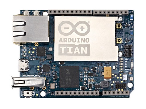
Fig. 2: The Arduino TIAN is a powerful development board designed specifically for the IoT. Image Source: Arduino.
TIAN is a powerful development board that was designed specifically for IoT applications and comes with an Atmel SAMD21 MCU based on an Arm Cortex-M0 processor clocking at 560 MHz. It is supported by 16 Mbytes of flash, 4 Gbytes of eMMC, and 64 Gbytes of DDR2 memory.
Wireless connectivity on the TIAN comes courtesy of a Qualcomm/Atheros AR9342 with a MIPS processor and dual-band 802.11b/g/n Wi-Fi and Bluetooth 4.0.
Its I/O support includes 20 digital GPIO, six analog input pins with a 12-bit analog-to-digital converter (ADC), one analog output with 10-bit digital-to-analog converter (DAC), serial, TWI, SPI, Ethernet, and support for the vast Arduino Shield collection.
In operation, the TIAN acts as a server and provides an OS-like interface through a browser on a connected computer, providing a window and menu interface for configuring the board. For development, the board supports Arduino IDE, a relatively mature integrated development environment.
The TIAN runs Linino, a complete Linux system for the IoT space, which is based on the OpenWRT-based (GNU/Linux) OS designed for embedded devices. If a design takes off, it’s hypothetically possible to port code from the TIAN to a custom PC board using the same or similar processor. So for embedded projects, especially for the IoT, the TIAN is a good place to initiate a design idea.
Given the importance of wireless connectivity, Wi-Fi support has been added to the widely used Arduino Uno via an integrated ESP8266 Wi-Fi module.
Note that Arduino has the oldest and most extensive support community, with countless projects, Arduino Shields, different OSes, code, tutorials, and more. When it comes to straight non-graphical embedded development, Arduino bubbles quickly to the surface of options.
BeagleBone Black Wireless is up for full-on embedded designs
For newbies, the BeagleBone Black Wireless (BBBW) requires a bit more programming skill, but it comes with a lot more connection points: up to 92 connections on two 46-pin headers, the majority of which can be used. Typically, these headers are used to expand the functionality of the BeagleBone using “BeagleBone Cape” expansion boards. These are comparable to Raspberry Pi HATs or Arduino Shields.
Its connectivity also sets the BBBW apart from the competition, including three I2C buses, CAN bus, SPI bus, five serial ports, 65 GPIO pins, seven analog inputs, eight PWM outputs, four timers, 1x USB 2.0 port, integrated 802.11b/g/n, and Bluetooth 4.1, plus BLE (Fig. 3 ). There is also non-operating-system-based support for peripherals via Texas Instruments StarterWare Libraries.
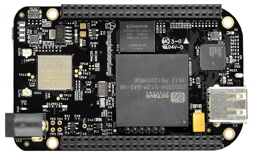
Fig. 3: The BeagleBone Black Wireless (BBBW) is a bit advanced for beginners but is very suited to embedded-system designs and can be run “out of the box.” Image Source: BeagleBoard.org.
Right out of the box, the BBBW’s 4-Gbyte eMMC flash is loaded with Debian Linux, so users can turn it on and start developing on it immediately. This is typically done through SSH on the BBBW’s USB port to a computer via Amazon Web Services’ (AWS) Cloud9, a cloud-based IDE. However, Android, Ubuntu, and many other Linux-based OSes are supported through third parties.
The BBBW’s main chip is the Octavo Systems OSD3358, a system-on-chip that combines an AM335x 1-GHz Arm Cortex-A8 core, a SGS530 3D graphics accelerator, a NEON SIMD engine, 2x PRU 32-bit 200-MHz microcontrollers, and 512 Mbytes of DDR3 RAM. Added storage is provided via 4 Gbytes of 8-bit eMMC flash and a microSD card slot.
BBBW has a robust community on par with the Raspberry Pi. The enthusiastic community provides a glut of projects, code examples, and hardware expansion. Based on the power and IO, BeagleBone has been chosen as the central control unit for many production CNC machines, which is a testament to the stability of this platform.
Hardkernel matches Samsung Exynos to Odroid
For hackers, makers, or developers looking for something different, try the ODROID-XU4 from Hardkernel (Fig. 4 ). The board is generating a lot of interest for IoT applications, as well as cluster computing, robotics, cloud computing, and even gaming.
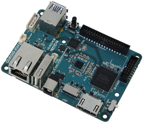
Fig. 4: The OROID-XU4 from Hardkernel matches a powerful 2-GHz Samsung Exynos5422 processor and Mali-T628 GPU to the Odroid environment. Image Source: Hardkernel.
The board itself is comparable to a small PC and is based on a Samsung Exynos5422 8-core processor (four Arm Cortex A15s and four Arm Cortex A7s) running at 2.0 GHz. This is supported by 2 Gbytes of LPDDR3 RAM and a Mali-T628 GPU. The extensive I/O includes a 30-pin GPIO header along with a 12-pin header for I2C and I2S connections. Wireless communication isn’t on-board but instead is provided using a custom IEEE 802.11ac/b/g/n 1T1R WLAN adapter that connects to the USB port.
Expandability is a bit different for these boards. Odroid does have a line of “Shields,” not to be confused with Arduino Shields that expand the functionality of the board. At the risk of confusing things further, there are Odroid Shields that will adapt the board for Arduino Shield and Raspberry Pi HATs.
Hardkernel itself offers an online support community with video tutorials and a plethora of open-source software located on the ODROID Wiki. Although this is the most expensive board here at $69, it is also the most powerful — processing heavy applications makes Odroid the first choice. However, at the time of this writing, it is out of stock at Hardkernel.
DECA brings DIY with an FPGA twist
It’s good to experiment with programmable logic with their cost and power consumption dropping and the tools getting easier to use. And it’s something completely different. With that in mind, try Arrow’s DECA. This was designed in collaboration with Altera and TI as an easy way to start using CPLDs and FPGAs, all in a tiny development board (Fig. 5 ).
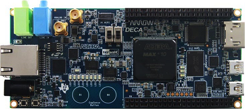
Fig. 5: The DECA development kit guides DIYers gently into more esoteric world CPLDs and FPGAs while providing designers with a fast path to implementing reconfigurable logic ideas. Image Source: Arrow Electronics.
The DECA comes with a MAX 10 FPGA with two multichannel ADC blocks, temperature sense diode, on-chip-RAM, and flash memory, microSD socket, accelerometer, various inputs, proximity/ambient light sensor, and one MIPI camera input. The board can output video through an HDMI interface. USB 2.0 OTG, 10/100-Gbits/s Ethernet, SDHC, and MIPI CSI-2 round out the board’s port options, while communications are handled by an Arrow Bluetooth Low Energy/Wi-Fi BeagleBone Cape.
For development, the DECA uses “The Platform Designer,” a system integration tool. Installed on a host computer, the software provides a proprietary graphical programming environment to simplify development.
Arrow provides an extensive online support community with design tools and apps for developing, designing, and programming to help kickstart FPGA development.
Advertisement
Learn more about Electronic Products Magazine


