Separate input and output power supply voltage connections enable power increases due to maximum output voltage swings
BY JOE KYRIAKAKIS
Cirrus Logic/Apex Precision Power
Austin, TX
http://www.cirrus.com
Due to the typical circuit topologies found in the output stages of power operational amplifiers, the output voltage swing may be limited to as much as 12 V less than the applied power supply voltage.
The discussion that follows illustrates one of several practical techniques that can significantly increasing efficiency by driving the output closer to the rail voltages using power op amps with special characteristics. Using these techniques can enhance power output by as much as 50%.
Some power op amps have two sets of power supply terminals, enabling the user to apply a separate higher-voltage supply to the input stages of the amplifier, while the output stage is set to a lower voltage. For example, the power op amp depicted in Fig. 1 uses this arrangement to achieve a “close-to-rail” voltage swing since the output devices, usually enhancement-mode MOSFETs, are driven close to saturation by the higher voltage (Vs ) available to drive the gates.
This arrangement allows the user to apply a higher power-supply voltage to the input circuitry than the supply voltage applied to the output stage. The voltage difference is usually between 5 and 15 V, which enables the output devices to be driven close to saturation. If this increased voltage swing is not needed, the input and output power supply pins are connected to provide equal supply voltage to the input and output stages.

Fig, 1. Some power op -amps have two sets of supply terminals enabling the user to apply a separate higher- voltage supply to the input stages of the amplifier, while the output stage is set to a lower voltage.
The power amplifier used in Fig. 1 has separate pins for Vb (the input stages) and Vs (the output stages) so that the designer can tie them together or power them separately, as discussed below.
Referring again to Fig. 1, the MOSFETs, Q4 and Q12 , deliver a maximum output current of 10 A to the load. In most applications +Vb and +Vs are connected together.
Since Q4 is an enhancement-mode device, the gate voltage must be at least 10 V higher than the source voltage to achieve the lowest source-to-drain voltage. (In the case of Q12 the gate voltage must be 10 V lower.) This means that the maximum output voltage will be at least 10 V lower than Vs .
By applying a higher voltage to Vb , the Q4 gate voltage is driven to a higher potential than Vs , forcing a higher Q4 source voltage. As indicated in the power amplifier datasheet, www.cirrus.com/en/pubs/proDatasheet/MP39U_G.pdf, the absolute maximum boost voltage, Vb , for this device is specified at 20 V higher than Vs , and the maximum boost supply current is 22 mA.
Isolated dc/dc converters
Isolated dc/dc converters may be used to supply the boost voltage. Many commercially available converters are suitable for handling this task. Figure 3 uses a pair of 3-W modules, available in either surface-mount or through-hole configurations. The 48-V input version offers an input voltage range of 36 to 72 V, and an isolated, regulated output of 12 V.
Two modules are required, one for the +Vb and one for the –Vb . The testing was performed with Vs set at 40 V. One module was powered from the +40-V supply, +Vs , and the other from the 40-V supply, Vs .
Since the outputs are isolated, other input power supply arrangements could be used, as long as the supply voltages are within the module’s operating input range. In the configuration shown in Fig. 2 , the voltage potential between the +Vb and the –Vb terminals is 52 V.
A pair of dc/dc converters connected as shown in Fig. 2 are powered by the 40-V power supplies that also provide the Vs voltages. The outputs of the converters are connected between the Vs and Vb of the power op amp terminals providing the required boost voltage.
To maintain a balanced load across the power supplies, the output of one converter in series is connected with the +Vs supply and common, and the second converter is connected between –Vb and –Vs . Because the outputs are isolated, any convenient power sources can be applied, as long as the total voltage applied to –Vb and +Vb does not exceed the specified input range.
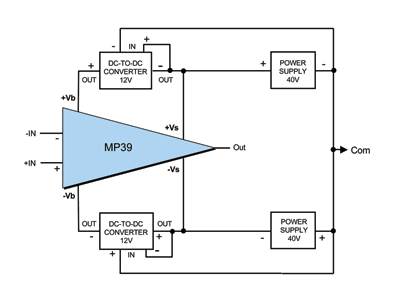
Fig. 2. A pair of dc/dc converters are powered by the 40-V power supplies that also provide the Vs voltages.
Off-the-shelf components
It is possible to develop a low-cost dc/dc converter by assembling off-the-shelf components readily available through common source distributors. The schematic in Fig. 3 depicts a converter designed specifically to provide the Vboost for any power op amp that features separate power pins for the input and power stages.
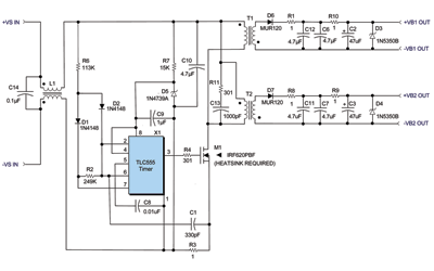
Fig. 3. This converter can be employed to supply the boost voltages (+Vb and Vb ) necessary to increase the output swing.
Note that transformers T1 , T2 , and the inductor L1 are Coiltronics part numbers, as identified in www.cirrus.com/en/pubs/appNote/Apex_AN48U_1.pdf, and are available from Cooper Bussmann. Because the two outputs are totally independent, a single converter will supply both the plus and minus Vboost .
The input voltage range is specified from 20 to 100 V to allow additional flexibility. The converter’s switching frequency is approximately 20 kHz and exhibits very low radiated and conducted noise components, assuming the circuit layout and ground scheme are given careful attention.
Transformer L1 is a common-mode filter that rejects common-mode noise due to the switching that occurs in the timer X1 , preventing it from feeding back to the VS source voltage. The snubber circuit, comprising of capacitor C13 and resistor R11 , counteracts ringing that would otherwise occur in transformers T1 and T2 . Full details regarding the components employed in this circuit can be found in www.cirrus.com/en/pubs/appNote/Apex_AN48U_1.pdf.
A 200-W op amp driving an 8-Ω resistive load
In Fig. 4 , a power op amp was configured as an inverting amplifier with a gain of 5, and driving a resistive load of 8 Ω. The value of the compensating capacitor CC, 220 pF, complies with the recommendation specified in the amplifier’s data sheet for a gain of 3 or more, and less than 10.
The power supply voltage, Vs , was set to ±40 V. The boost voltages, +Vb and –Vb , are set at 12 V. The power delivered to the load is 200 W peak with the boost voltage applied, and a much lower 144 W peak delivered with no boost voltage.
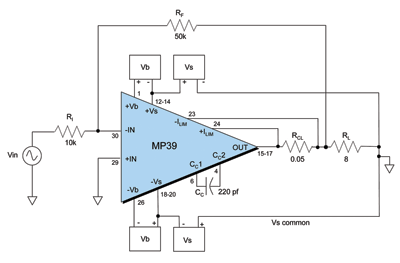
Fig. 4. This circuit configured with an inverting gain of 5, Vb of 12 V and a Vs of 40 V.
This significant increase in realized power can be important in high-efficiency applications. The MP39 datasheet limit for output voltage swing is ±8.8 V. This means that output clipping could occur at 31.2 V without applying the boost voltage.
The responses both with and without the boost circuitry are shown in the graphs in www.cirrus.com/en/pubs/appNote/Apex_AN48U_1.pdf. ■
Advertisement
Learn more about Cirrus Logic


