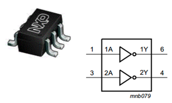
The 74LVC2G04GW is a dual inverting buffer that features a 5 V tolerant inputs for interfacing with 5 V logic. It operates with a wide supply voltage range from 1.65 V to 5.5 V at a specified temperature of -40 °C to +125 °C. The device is surface-mounted with a plastic packaging having 6 leads.
This device is fully specified for partial power-down applications using IOFF. The IOFF circuitry disables the output, preventing the damaging backflow current through the device when it is powered down.
Features
- Wide supply voltage range from 1.65 V to 5.5 V
- 5 V tolerant inputs for interfacing with 5 V logic
- High noise immunity
- Complies with JEDEC standard:
- JESD8-7 (1.65 V to 1.95 V)
- JESD8-5 (2.3 V to 2.7 V)
- JESD8B/JESD36 (2.7 V to 3.6 V)
- ESD protection:
- HBM JESD22-A114F exceeds 2000 V
- MM JESD22-A115-A exceeds 200 V
- ±24 mA output drive (VCC = 3.0 V)
- CMOS low power consumption
- Latch-up performance exceeds 250 mA
- Direct interface with TTL levels
- Inputs accept voltages up to 5 V
- Multiple package options
- Specified from -40 °C to +85 °C and -40 °C to +125 °C
Advertisement
Learn more about NXP Semiconductors


