Today’s consumers carry their portable devices (PDs) like smartphones, tablets, and media players everywhere. But when you bring these PDs into an automobile, they may not charge quickly or charge at all, especially the more recent power-hungry PDs. Additionally, there are not even enough USB ports for all the passengers, leaving consumers competing over the single USB port to charge their device. With USB expected to reach into almost 100% of automotive infotainment systems, automotive OEMs and their suppliers need to address this need.
Automobile passengers want a full-featured, rapid-charging USB access port in even the lowest-cost vehicles, and they want more of them. Low-cost USB car chargers are not the solution because they introduce radio interference (RF) into the vehicle. Automotive OEMs are very much aware of these PD charging and RF inference problems. They are working hard to find the most reliable, lowest cost way to upgrade the existing USB port and add more USB charging ports to each vehicle.
Traditional USB solutions required four or five discrete components to solve the problems. This article discusses a new dc/dc converter with a smart USB switch that leverages tight integration to provide automotive-specific USB power, USB charge enumeration, port protection, and solves recent problems with higher PD charging current. It makes USB practical for automotive manufacturers and consumers alike.
The USB challenges for automobiles
We will begin with the main challenge, which is the current requirement. The USB charging current requirement for PDs has been growing steadily as each device’s battery capacity has increased. Vehicle USB ports have historically been limited to 500 mA, but new PDs require up to 1, 1.5, or even 2.1 A at 5.0 V to charge rapidly.
Now, let’s talk about distance. Because the National Highway Traffic Safety Administration (NHTSA) advises against a radio front-access USB port, the vehicle’s main USB port is typically located in the glove box, beneath the radio/center stack, or in the armrest storage compartment area between the seats. This USB port location can be anywhere from 30 cm to 3 m from the radio and is connected by a permanent, captive USB cable. Once the PD is connected to this remote USB port, the PD draws current and attempts to charge. The current through the resistance of the USB VBUS (+5 V) power line and the USB ground line results in a voltage drop (I × R) across the captive cable. When the voltage at the PD is below the USB specification, it causes reduced charging current and a longer charge time (see Fig. 1) . For example, a 500-mΩ cable can cause a 750-mV drop for a PD charging at 1.5 A, thus reducing the voltage at the PD to 4.25 V.
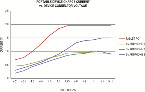
Fig. 1: Four of today’s leading smartphones and tablets were tested for performance. When the voltage at the PD is below the USB specification, it causes reduced charging current and a longer charge time.
Finally, there is an RF problem. To have more USB charging ports, consumers bring cigarette-lighter-style USB car chargers into the vehicle. OEMs cannot control the quality, operating frequency, or topology of the dc/dc converter in those simple chargers. Not surprising, a poorly designed dc/dc converter in these USB car chargers can jam the AM receiver, create static for the FM receiver, interfere with the touchscreen of a smartphone, and reduce sensitivity of embedded vehicle RF functions such as GPS and passive-entry systems. All of these problems can cause a poor consumer and OEM brand experience.
Design approaches to meet these USB challenges
The permanent USB captive cable discussed above dictates the OEM architecture and solution cost for the main USB port to the radio. To achieve rapid charging, three general solutions have surfaced:
1. Use larger-gauge cable/connectors for the VBUS and GND power path in the USB cable.
2. Add another self-powered USB hub module at the consumer access point.
3. Design an “intelligent” chip-based solution with correction of the USB captive-cable voltage drop by increasing the USB voltage in the radio to hold 5 V at the end of the cable.
Architectural solution number 3 is by far the lowest-cost system solution, but it must be executed correctly for optimal performance. Today’s typical implementation is a three-chip solution.
A new, fourth solution resolves these automotive USB challenges and keeps the costs, size, and weight lower than other existing solutions. The new design uses the MAX16984 step-down dc/dc converter with integrated USB protection/host charger adapter emulator. Let’s take a closer look at this new approach.
Resolving the RF interference and cable drop problems
To prevent the RF interference caused by consumer-grade USB car chargers, more in-vehicle USB ports should be integrated into the car. The dc/dc converter used in these in-vehicle USB ports must have key performance features. For starters, it needs a fixed-frequency, pulse-width modulation (PWM) topology that provides well-predicted switching harmonics and EMI characteristics. To avoid the AM band, designers can then either switch below 550 kHz or above 2 MHz to avoid interfering with the tuner. If below AM, the dc/dc converter must have an external digital SYNC input to allow the microprocessor to set the converter’s switching frequency and to avoid the AM tuner frequency. If above AM, no AM interference occurs and is the preferred method. However, above 2 MHz, the dc/dc converter will have higher switching losses, faster switching times, and wider bandwidth.
For optimal FM reception, it is necessary to avoid both the 10.7-MHz IF frequency and to eliminate harmonics in the FM band itself. Switching above the AM-band makes it easier to avoid the 10.7 MHz because the harmonics are spaced farther apart. Using 2.2 MHz is a preferred operating frequency because the fourth harmonic is 11 MHz, placing it 300 kHz from the 10.7-MHz IF. To avoid the FM frequency itself, the dc/dc converter needs an internal spread-spectrum oscillator. This dithers the 2.2 MHz operating switching frequency so that harmonics in the FM band do not interfere with the main FM carrier signal (see Fig. 2 ).
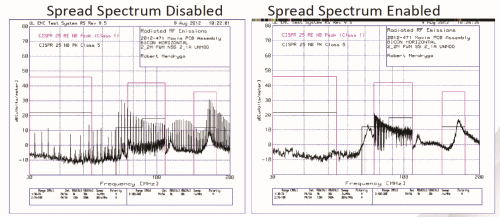
Fig. 2: Spread spectrum enabled/disabled for the MAX16984.
It is critical that the dc/dc converter maintain a fixed frequency at no load (zero-dc USB current to the PD). This eliminates the low-frequency harmonics caused by SKIP (burst) mode operation and prevents them from interfering with the smartphone’s touchscreen or with the 100-kHz passive-entry system. To maintain fixed-frequency operation at no-load current, the dc/dc converter must have an internal low-side synchronous FET and a control-loop topology to shuttle current into, and out of, the capacitor on the converter’s output when no dc USB load current is present (see Fig. 3 ).
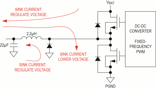
Fig. 3: The MAX16984 sourcing/sinking supply.
There is a method to increase the USB voltage in the radio and overcome the voltage drop of the captive USB cable. You need to sense the DC USB load current, pass it through a transimpedance amplifier (TIA), and adjust the dc/dc converter’s main control loop:
Vout = Vnoload + Iload x Gi x Gv (Eq. 1)
To achieve USB certification and keep the voltage at the PD between 4.75 and 5.25 V at up to 1.5-A of load current, the topology, total accuracy, and bandwidth of this method are all critical.
In this architecture, the voltage at the PD is (see Fig. 4 ):
Vpd = Vout – Iload x Rcable ——› Vpd = Vnoload + Iload x Gi x Gv – Iload x Rcable (Eq. 2)
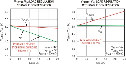
Fig. 4: Data from the MAX16984 show how 5 V is maintained for the PD.
By analyzing the error sources, it can be shown that both the USB current requirement and the captive-cable tolerance establish the remaining allowable implementation errors:
250 mV ≥ ΔVnoload + Iload x Δ(Gi x Gv) – Iload x ΔRcable (Eq. 3)
Given Equation 3, a 1.5-A load requirement and a typical OEM cable tolerance of ±17%, we can conclude:
• Cable tolerance sets the remaining allowable error in the system.
• The remaining accuracies for the dc/dc converter output voltage and the TIA will limit the maximum cable length. The less accurate the method, the total resistance and the shorter the captive cable (see Fig. 5 ).
• The dc/dc converter must have a very accurate no-load output voltage because it is translated directly to the PD regardless of load current. Accuracy of 1% or better is required.
• The TIA integrated in the MAX16984 is trimmed and very precise. In contrast, the tolerances can stack up quickly when using a dc/dc converter with a discrete TIA.

Fig. 5: Nominal cable properties vs. total amplifier error
There is, finally, a critical, often overlooked, feature of the dc/dc converter. As noted above, it must have a sourcing and sinking topology with a wide, closed-loop bandwidth (> 200 MHz). (See Fig. 3 .) This topology is needed to quickly increase (source current) and quickly decrease (sink current) the output voltage of the dc/dc converter during load current steps. In addition, the integrated TIA must also have a wide bandwidth. This converter design prevents any overvoltage transients from reaching the PD (see Fig. 6 ). Without this methodology, a 6-V pulse for 20 ms can be presented to the PD.
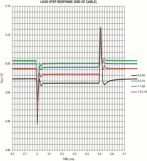
Fig. 6: Data show the MAX16984 the load step response at the end of the cable. This performance prevents any overvoltage transients from reaching the PD.
Achieving a robust automotive solution
With USB penetrating virtually all automobiles, vehicle OEMs need a full-featured, low-cost, rapid-charging USB port accessible to any consumer’s PD. Vehicles must have multiple, dedicated USB charging ports (charging only). And all this USB functionality needs to be in a small, highly reliable and integrated solution available in both the high-end and lowest cost vehicles.
A robust automotive solution requires extra ESD protection to safeguard the USB data lines from OEM extended ±25-kV requirements; an intelligent USB IF BC1.2 data enumerator to enable the PDs to charge rapidly; a USB data switch protector to isolate the transceiver USB data lines from shorts to the +5-VBUS line and shorts to GROUND; a wide operating voltage (4.5 to 42 V), fixed-frequency (no load to full load), sinking/sourcing +5-V dc/dc converter to prevent vehicle RF interference; a precise, captive-cable voltage-adjustment circuit to raise the dc/dc converter’s output voltage to maintain +5 V at the end of the captive USB cable; a precise dc current limit to protect the +5 VBUS from shorts to ground. And of course, the solution must use full AECQ-100-compliant components.
All these capabilities are integrated in a new dc/dc converter, the MAX16984 (see Fig. 7 ). This dc/dc converter will detect, supply, and protect the main USB power port and facilitate tiny additional USB charging ports in any automobile at an incredibly small form factor (see Fig. 8 ).
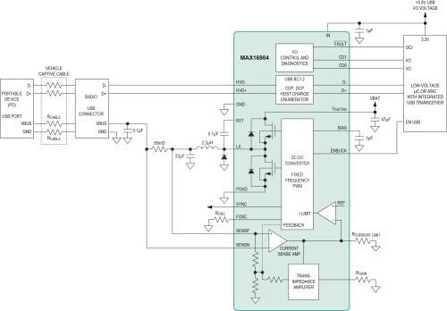
Fig. 7: System diagram and block diagram of the MAX16984.
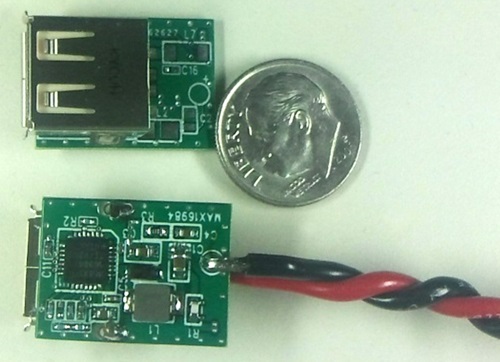
Fig. 8: Form factor for complete MAX16984 solution shown next to a U.S. 10-cent coin.
Automotive USB Performance and Cost Comparison
The automotive industry uses one of these four topologies (see Table ) to ensure efficient, fast charging of any PD from a vehicle’s main USB port. Methods 1 and 4 use the fewest number of components. Methods 2, 3, and 4 accommodate the higher voltage requirements of new PDs. Method 4 is the lightest, smallest, and lowest-cost solution today.
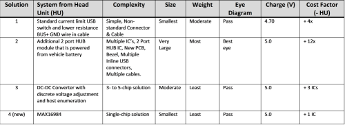
Table: USB charging performance and cost comparison
Advertisement
Learn more about Maxim Integrated


