By Brian Santo, contributing writer

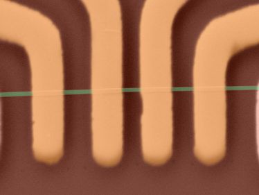
Image source: University of California Riverside.
The semiconductor industry is rapidly approaching the physical limits not only of silicon but also of copper, commonly used for IC interconnects. Engineers at the University of California at Riverside have demonstrated prototype devices using zirconium tritelluride (ZrTe3 ) that can conduct a current density 50 times greater than conventional copper interconnects.
Ideally, the use of some exotic material that can sustain high current densities — perhaps ZrTe3 — will enable the semiconductor industry to continue with silicon for a few additional device generations.
IC manufacturers relied mostly on aluminum for interconnects until about 20 years ago, when the industry moved to copper. Since copper is a superior conductor, less material was needed for the interconnects. As a practical matter, swapping the materials helped the industry continue to scale its circuitry. The switch also necessitated the development of new production equipment and processes. It was difficult and expensive, but because it enabled the industry to keep scaling silicon for another two decades, it was unquestionably worth the investment.
At today’s processing nodes, copper is running up against limits in current density — the amount of electrical current per cross-sectional area at a given point. As the industry attempts to continue scaling ICs down in size, transistors need higher and higher current densities to perform at the desired level. Copper and most other conventional electrical conductors tend to break due to overheating or other factors at high current densities, presenting a barrier to creating increasingly smaller components, explained UC Riverside researchers.
So the industry has been exploring other materials as potential replacements for copper, just as copper once replaced aluminum.
Some companies are already using alternatives to copper at the smallest processing nodes. It’s been reported that both Intel and GlobalFoundries are using cobalt for some interconnects at the 10-nm node. Cobalt is better than copper but not by much.
The industry is also looking at more exotic alternatives that can provide significantly higher current densities. Notable among them is graphene, which was recently discovered to be superconducting . Graphene is considered a two-dimensional (2D) material in that it can be created in sheets that are a single atom-layer thick. Researchers have been able to create what they’re calling nanoribbons of graphene down to a few atoms wide.
But if 2D is good, wouldn’t 1D be better? The question sparked an investigation into the potential use of materials that can be fabricated as single-atom strands. They’re not technically 1D, but they are as close as you can get. When researchers are being scrupulous about terminology, they call single-strand materials “quasi-one-dimensional.”
The research at UC Riverside is led by Alexander A. Balandin, a professor of electrical and computer engineering. He and his team have discovered that ZrTe3 has an exceptionally high current density that far exceeds that of any conventional metals like copper.
Copper has a current density of 2 MA/cm2 to 3 MA/cm2 . Zirconium tritelluride has a current density of about 100 MA/cm2 , according to a UC Riverside research paper.
Thus far, UC Riverside researchers have been cutting nanoribbons of ZrTe3 from sheets of the material, but the team is confident that it will be possible to process the material as 1D strands. ZrTe3 nanoribbons could be made into either nanometer-scale local interconnects or device channels for components of the tiniest devices, said UC Riverside.
“Conventional metals are polycrystalline,” said Balandin. “They have grain boundaries and surface roughness, which scatter electrons. Quasi-one-dimensional materials such as ZrTe3 consist of single-crystal atomic chains in one direction. They do not have grain boundaries and often have atomically smooth surfaces after exfoliation. We attributed the exceptionally high current density in ZrTe3 to the single-crystal nature of quasi-1D materials.”
While the bulk resistivity of the 1D is higher than that of copper, Balandin told Electronic Products, it is expected that it will not degrade as fast as the resistivity of copper does with a decreasing cross-section area.
Thus far, ZrTe3 quantum wires exhibit current densities higher than reported for any metals or other 1D materials — and almost reach the current density in carbon nanotubes and graphene.
Balandin said that his team has tried several other materials and that tantalum triselenide (TaSe3 ) also has promise as a semiconductor interconnect.
The team has produced a prototype that demonstrates the ability to create ZrTe3 nanoribbons on a silicon/silicon-dioxide substrate, but Balandin told Electronic Products that he and his team have not yet made a functional device.
If the current density of ZrTe3 is sufficient for the next few nodes of semiconductor manufacturing, being 1D might be more of an advantage than being superconducting. The practicality of using ZrTe3 would also be predicated on how well it can be added to the silicon manufacturing process. The UC Riverside researchers report that they are developing a process to grow ZrTe3 nanoribbons directly on silicon wafers.
When asked about the prospect of using ZrTe3 with standard CMOS production equipment, Balandin said, “The project is funded by the Semiconductor Research Corporation (SRC) with industrial liaisons from Intel Corporation. At this point, industry is open for any material that can deliver high current density in small cross-sections and with acceptable resistance. Our materials have shown record-high current density.”
Advertisement
Learn more about Electronic Products Magazine


