University of Utah engineers have developed an ultracompact beamsplitter, the smallest ever created, for dividing light waves into two separate channels of information. This breakthrough technology brings researchers a step closer to producing silicon photonic chips that compute and move data with light instead of electrons, at speeds millions of times faster than anything on the market today.

Beyond computers and mobile devices, though, silicon photonics can also increase the power and speed of machines like supercomputers, data centers, and the currently-in-development computer systems for autonomous cars and drones with collision detection.
“Light is the fastest thing you can use to transmit information,” says Electrical and computer engineering associate professor Rajesh Menon, who worked on this project with a team of colleagues. “But that information has to be converted to electrons when it comes into your laptop. In that conversion, you're slowing things down. The vision is to do everything in light.”
It should be noted that at present, photons of light are already tasked with carrying information over the Internet via fiber-optic networks. The slow-down occurs once a data stream reaches its home or office destination, as it is at this point that the photons of light must be converted to electrons before a router or computer can handle the information. This bottleneck, if you will, could be eliminated if the data stream remained as light within computer processors.
“With all light, computing can eventually be millions of times faster,” says Menon.
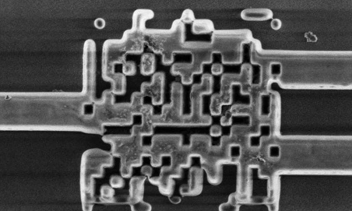
In order to achieve this new benchmark, Menon and his team created a much smaller polarization beamsplitter on top of a silicon chip that can split guided incoming light into its two components. In terms of footprint, an old beamsplitter would take up, at minimum, 100 microns by 100 microns of space. The new device created by the group is just 2.4 microns by 2.4 microns, or one-fiftieth the width of a human hair, and at the very cusp to the limit of what is physically possible.

Overhead view of a new beamsplitter for silicon photonics chips that is just 2.4 microns by 2.4 microns in size.
Given its incredibly minuscule physical presences, the beamsplitter would be just one of a whole bunch of passive devices placed on a silicon chip to direct light waves in different waves. And by shrinking them down in size, engineers can cram millions of these devices on to a single chip.
Beyond the obvious improvement in processing speed, the team’s design is pretty cheap to produce as well. This is due to the fact that it uses existing fabrication techniques for creating silcon chips. What’s more, because photonic chips move photons instead of electrons, mobile devices built with this technology would require much less power which, in turn, would lead to longer battery life; it also means these devices will generate less heat.
Supercomputers using silicon photonics are already in development at companies like Intel and IBM, but they use hybrid processors that remain partly electronic. Menon and his team believe their beamsplitter can be used in these computers in the next three years. They add that data centers that require faster connections between computers could also implement the technology soon.
Read the published report, entitled “An integrated-nanophotonics polarization beamsplitter with 2.4 x 2.4µm2 footprint”, in Nature Photonics.
Via the University of Utah
Advertisement
Learn more about Electronic Products Magazine


