BY CHAD MARAK, director of semiconductor business development,
Littelfuse,
www.littelfuse.com
As the universe of portable, wireless, and wearable devices expands, so does the potential for field failures due to electrostatic discharge (ESD) exposure. The most common cause of ESD is friction between two dissimilar materials, causing a buildup of electric charges on their surfaces. Typically, one of the surfaces is the human body itself, and it is not uncommon for this static charge to reach a potential as high as 15,000 V. At 6,000 static volts, an ESD event will be painful to a person. Lower voltage discharges may go unnoticed, but can still cause catastrophic damage to electronic components and circuits. Every new access point on an electronic device multiplies the risk of damage by forming electrical paths for the high potential currents into the device itself. The survival of these sensitive electronics depends on comprehensive circuit protection.
When performing an ESD survival analysis on a typical handheld device, every data or power interface can represent a gateway into the system for ESD. These necessary breaks in the insulation and shielding in the body of the unit are also opportunities for transient incursions. The goal of any ESD mitigation effort is to “clamp” or limit the inbound ESD transients to non-destructive levels. Silicon transient voltage suppression (TVS) diodes and diode arrays are among the most effective ESD protection technologies available.
Earphone jacks
An ESD discharge in the vicinity of an earphone port may pass into the interior of the device and arc via the speaker circuit. Because the signals found on this circuit are very low speed (
Keypad, pushbuttons, switches
These simple components can provide a path for ESD to the circuit board if the transient arcs from the switch structures to the circuit board. Because they are essentially dc lines, a suppressor with high capacitance such as 30 pF is recommended.
Power port
This low voltage input is used to charge the battery and to provide direct power to the circuits. As a true dc circuit, a high-capacitance suppressor is recommended.
I/O port – Edge connector
The primary factor to consider for protecting this signal port is the data rate of the signals. As data rates increase, it is crucial to consider the capacitance of the chosen suppressor so as not to introduce any signal integrity issues into the system. For example, circuits in this port running at low speeds can be protected with higher capacitance TVS diode arrays or something with tens of picofarads.
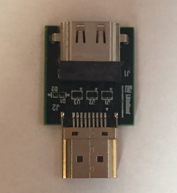
For extremely high data rate protocols such as USB3.0 or HDMI 2.0, choose suppressors with very little capacitance so that the system is able to transmit and receive the data with no loss of signal quality (due to the protection device).
TVS diode arrays provide high levels of protection against ESD, electromagnetic interference (EMI) and lightning. These devices work in two ways. First, they absorb transients with diodes, to steer the current, and then, an avalanching or zener diode clamps the voltage to an acceptable level. During over-voltage conditions, the device must have a low clamp voltage at the specified current waveform to protect sensitive ICs and ports. In normal operation, the reverse standoff voltage must be higher than the equipment supply/working voltage, with low leakage current to prevent power supply loading. The device capacitance must be low enough to reduce input signal distortion. The device package must have a small footprint and low height to save space in high density board layouts. The device must withstand multiple ESD pulses as specified in the IEC 61000-4-2. Other key characteristics such as number of lines of protection, ESD immunity, and footprint also need to be considered.

TVS diode arrays provide high levels of protection against ESD, EMI, and lightning
Weighing all these considerations in order to choose the most appropriate TVS Diode Array for an application just became a lot easier with the Littelfuse iDesign Online Simulation and Product Selection Tool. Circuit designers can enter the system and device parameters, then choose up to three TVS diodes for comparison. A built-in simulation tool allows making a quick comparison of how they will perform in the application without the need to build prototypes. For free access to the iDesign online tool, register at www.littelfuse.com/iDesign. To learn more about how the iDesign online tool works, view the Littelfuse iDesign Tutorial Videos.
Advertisement
Learn more about Littelfuse


