BY KURT SMITH, Reliability Manager, and RONALD BARR, VP of Quality
Transphorm
www.transphormusa.com
Extensive reliability testing is an essential phase of any new product or technology. Transphorm utilizes standard JEDEC qualification testing prior to commercializing its GaN (gallium nitride) FETs to ensure that the quality of the devices will meet customer expectations for reliability. However, since the JEDEC tests were originally developed for silicon technology, Transphorm’s testing has gone beyond the minimum requirements of JEDEC testing by running tests on a much larger number of devices than the minimum required. In addition, aggressive accelerated life testing was also performed.
JEDEC qualification
JEDEC testing typically uses relatively large numbers of devices and applies a fairly modest level of stress to those devices. The tests are designed to give a lot of information about infant mortality and a limited amount of information about the constant failure rate portion of the well-known bathtub curve, but virtually nothing about the wear-out failure portion. By passing this suite of tests, Transphorm has demonstrated that its GaN products are free from any of the typical defects that can have a negative impact on short-to-medium-term reliability. Since JEDEC-type testing does not provide the required resolution to be able to predict lifetime in the field, more aggressive accelerated life testing becomes the methodology of choice.
High-temperature switching operation test
During normal operation, the devices were exposed to many of the JEDEC test conditions simultaneously. The high-temperature operating life test (HTOL) mimics hard switching conditions in applications and provides insight into possible interactions affecting reliability. The tests used standard parts operating as the main switch in a boost converter. The devices were run at a 175°C junction temperature, which is higher than the 150°C reported in the datasheet. The higher temperature provides a minor acceleration of the test, but higher temperatures result in the degradation of external components, thereby limiting the maximum junction temperature to 175°C.
Fig. 1 shows conversion loss of the devices over the life of the HTOL. Degradation of the solder contacts and external components in the circuit account for the increase in conversion loss after 2,000 hours; the devices showed no significant change in performance when measured after the HTOL. While this test does not predict lifetime, the GaN devices are robust for extended times at the maximum rated temperature in actual operating conditions.
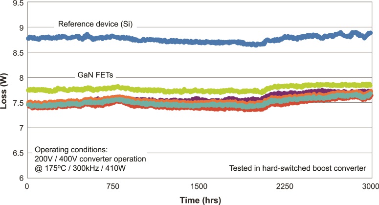
Fig. 1: Loss plot for HTOL of seven 600-V-rated GaN-on-Si FETs and a reference device to 3,000 hours at Tj = 175°C.
Wear-out testing
Wear-out is the predicted lifetime or point that the parts will begin to fail at an increasing rate due to aging lifetime projections, which depend on understanding and modeling the wear-out process and are based on accelerated testing to failure. The operating conditions of a power switch allow for separation of the major stress factors.
Fig. 2 shows failure times plotted on a graph of log time versus 1/temperature in Kelvin (Arrhenius plot). Each set of devices is represented by a mean time to failure (MTTF) point (triangle) or the point at which 50% of the devices are failed. The slope of the line fitted to the MTTF points provides the physical understanding of the degradation mechanism, through the activation energy (Ea ). In this testing, Ea is 1.84 eV, which is in good agreement with the values reported in the literature. The line also predicts the lifetime-at-use temperatures such as 423°K (150°C), which is >1 x 10⁸ hours.
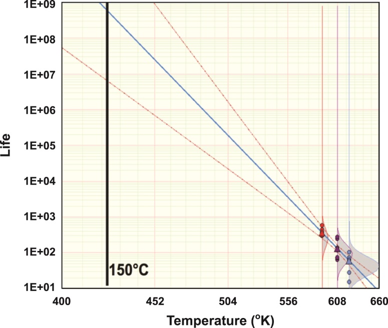
Fig. 2: Arrhenius plot showing MTTFs for the three temperatures (in °K) and lifetime extrapolation including 90% confidence limits.
The statistical validity is demonstrated both by the range of the failure points and by the 90% confidence limits shown by the dashed lines. The small range of values around the MTTF point provides confidence that the expected failure mode is being represented. The lower limit of that range is still >1 x 10⁶ hours or >100 years at 150°C.
The first report of GaN high-field-related lifetime is >1 x 10⁸ hours at 600 V. For the high-field lifetime testing, three sets of standard 600-V production parts (GaN HEMTs cascoded with Si FETs) were biased in the off-state at high drain voltages of 1,050, 1,100, and 1,150 V. Device temperature was set at 82°C to match expected use conditions.
Fig. 3 shows a graph of the failure times versus voltage for one possible failure model: linear voltage time-dependent dielectric breakdown (TDDB). However, the reported prediction is based on a reciprocal voltage TDDB model that represents the most conservative lifetime, as shown in Fig. 4 . Similar to the Arrhenius plot of Fig. 2 , the small range of failure times around the MTTF points demonstrates the quality of the test. The 95% confidence limits (dashed lines) give a strong support to the projected lifetimes reported. The slope of the line provides the acceleration factor needed to provide a physical understanding.
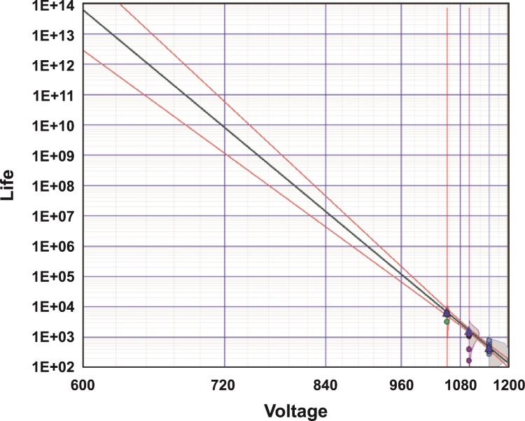
Fig. 3. Log time versus 1/V plot of high-voltage OFF state (HVOS) testing using a linear TDDB model for illustration of data integrity (projection may not provide the device lifetime).
Although the plots above are useful for understanding the reasons behind the devices failing, the use plots of Fig. 4 and Fig. 5 are more helpful in understanding the process lifetime and reliability. In each plot, all devices (including multiple sample sets) tested at accelerated conditions are projected back to a use condition based on the physical parameters determined from the plots above. The Weibull plot combines all of the devices into a single set and allows a more detailed understanding of the variability of the process as well as predicting device lifetime.
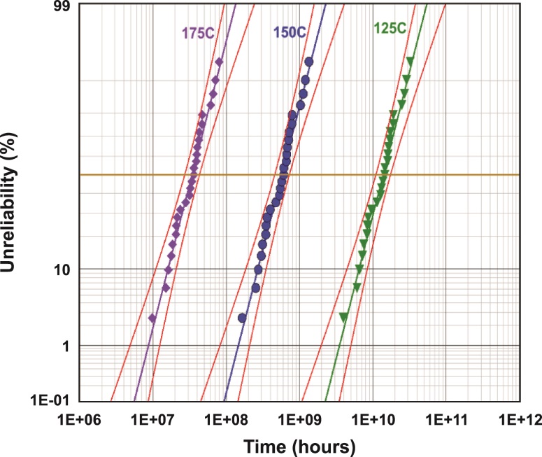
Fig. 4. Use plot of all HTDC device failures at three different use temperatures.
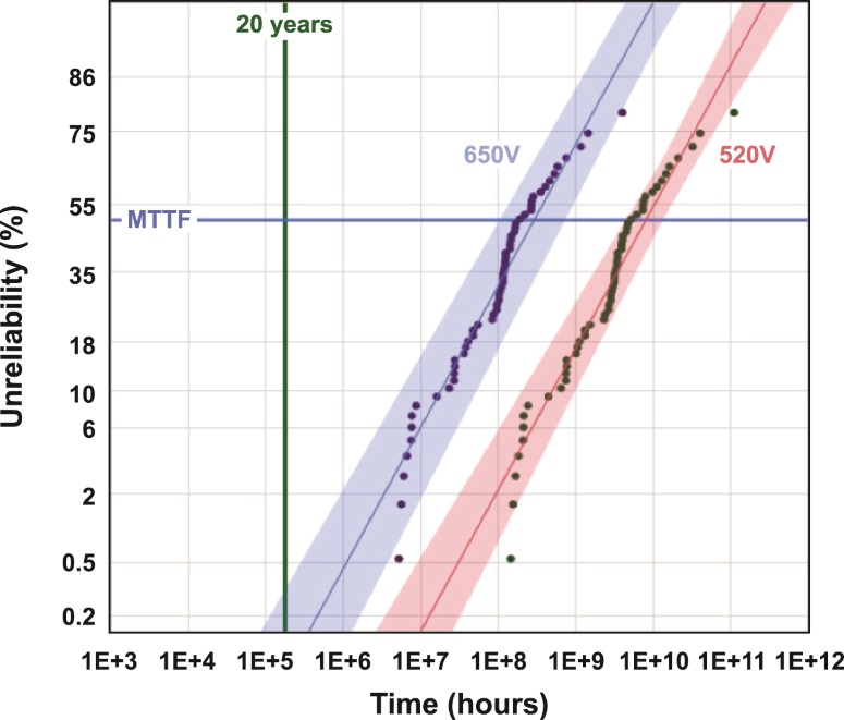
Fig. 5. Use plots based on voltage accelerated testing showing all failed devices during HVOS testing for the reciprocal field TDDB model.
The results in Fig. 5 are from high-field testing of sample sets across three lots. High-field lifetime at 650 V (or 520 V, as shown) can be directly taken from the plot, not only at 50% failures (>1 x 10⁸ hours), but also at low percentages such as 10% (~1 x 10⁸ hours) or 1% (~1 x 10⁷ hours). The relatively steep slope of the multiple sample sets shows the small variability of the process lot to lot as well as within a wafer. The 95% confidence limits provide assurance that the projected lifetime for 1% failures is >1 x 10⁶ hours. Additionally, the first failures do not form a significant tail. The lack of a tail indicates that the field-related FIT rate will remain low for the lifetime of the devices.
Similar to the field-related use plot, the temperature-related use plot of Fig. 4 shows median lifetime of >2 x 10⁷ hours at the peak-rated junction temperature of 175°C. The steep slope of the fitted line and the narrow 95% confidence limits show the small variability of the process. Device and test time availability contributed to limited sample sets, but the robustness of the high temperature results and the 1.8-eV activation energy that match reported values provide great confidence in the reliability of Transphorm’s products.
Use GaN with confidence
JEDEC-style testing and HTOL have demonstrated that the initial quality and robustness of Transphorm’s process to qualify GaN is sufficient for user applications. The projected mean lifetimes for both the on-state and off-state are greater than 1 x 10⁷ hours at nominal operating conditions, which exceeds known requirements. Since Transphorm’s GaN products are produced using the same methods and materials as silicon products, the reliability of GaN products should be indistinguishable from the reliability of silicon products.
Advertisement
Learn more about Transphorm


