Evaluating jitter tolerance in high-speed signals
To maintain signal and power integrity at 28-Gbit/s data rates, some important challenges must be resolved
BY HIROSHI GOTO
Product Specialist, Anritsu
www.anritsu.com
The rapid spread of cloud computing services and smartphones is causing a steady increase in network transmission capacities, so much so that the momentary traffic at some Internet exchanges is approaching 1 Tbit/s. As IT equipment counts increase to accommodate greater traffic, power consumption requirements pose an even bigger challenge.
Faster device integration data rates and transmission speeds are effective methods for increasing the amount of processed data while minimizing power consumption. Currently, the 28-nm processes being used can support data rates in the 28-Gbit/s band, effectively reducing power consumption per Gbit/s. To maintain signal and power integrity at 28-Gbit/s data rates, however, some important challenges must be resolved.
As frequency is increased, signal amplitudes are typically lower and bit periods significantly shorter. Therefore, impacts on amplitude or phase have a much greater effect on signal integrity, resulting in lower margins and a higher probability of errors. The physical length differences between signal paths, especially two sides of a different pair, become important to manage.
If noise of 100 mVp-p overlays a signal amplitude of 400 mVp-p, the threshold margin is reduced by as much as 25%. When a 25-Gbit/s signal is transmitted on a line of an FR-4 printed-circuit board (PCB) with a wiring length that differs by 10 mm, a phase difference of more than 1 bit occurs, due to a deviation of 70 ps for one 40-ps bit. This greatly affects signal integrity. Consequently, because it is difficult to maintain signal integrity for data rates in the 20-Gbit/s band, thorough simulation and verification is essential.
There are many physical phenomena, such as jitter, inter-symbol interference (ISI) and crosstalk, which contribute to reduce signal integrity. These phenomena cannot be eliminated completely at high data rates. Therefore, it is important to take into account the signal integrity reduction for both the transmitter circuit and the receiver circuit to ensure the quality of the output signal and receiver tolerance. Engineers must incorporate an analysis method that verifies the quality of the output signal and the receiver tolerance in terms of these phenomena, particularly jitter.
Measuring jitter tolerance
Signal quality analyzers (SQAs) have become a primary test tool to determine the jitter tolerance in these designs. The reason is that an SQA combines a pulse pattern generator (PPG) and a Bit Error Rate Tester (BERT), so it can generate a signal to inject into a device under test (DUT) and then determine the BER. However, to accurately test today’s high-speed designs, an SQA must be able to generate 28 Gbits/s signals and have the ability to measure every bit at that speed. Additionally, the analyzer should have certain features, such as wide frequency bandwidth, a low jittered output signal and excellent jitter transparent capability, to support high accuracy jitter tolerance testing.
For today’s high-speed designs, the ability to support jitter tolerance tests of various standards is critical, as well as measuring different types of jitter. Table 1 shows the various jitter types and their causes.
Table 1: Various jitter types and their causes
To effectively evaluate jitter reception tolerance, a DUT needs to receive a signal for which pseudo-imposition of jitter has been performed, then the bit-error rate (BER) must be measured and the resistance evaluated. An SQA can accomplish this, as the PPG can generate Sinusoidal jitter (SJ) to simulate deterministic jitter (DJ) in a test environment (see Fig. 1 ).
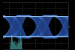

Fig. 1: To achieve the SJ component of the data waveform (a) and its spectrum distribution (b) shown, the SQA used must have as little intrinsic jitter as possible. In this instance, the intrinsic jitter of the SQA is 5 ps peak-to-peak.
To accurately measure BER in high-speed designs, the BERT must be able to analyze every bit at 28 Gbits/s. Many BERTs cannot view every bit at such a high speed. If the BERT is unable to view every bit, many more samples must be taken, which takes considerably more time and increases the cost of test. Equally important, repeatability and accuracy is lessened if the BER cannot test every bit at 28 Gbits/s (see Fig. 2) .
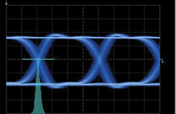

Fig. 2: The jitter histogram (a) and spectrum distribution (b) of RJ on a 28-Gbits/s signal can be obtained rapidly, repeatably, and accurately using an SQA.
4-tap pre-emphasis needed
An additional consideration is to ensure that today’s high-speed signals are transferred through PCBs with the slightest bit of attenuation. To help achieve this design goal, many backplane and interconnect interfaces use pre-emphasis technology to maintain the necessary eye opening by correcting the level attenuation.
Engineers can use a 4-tap pre-emphasis converter with an SQA to support easy changes to the pre-emphasis waveform amplitude and the offset of each tap. This helps ensure effective evaluation of the characteristics of high-speed interfaces below 10 Gbits/s requiring pre-emphasis signals, such as PCIe, USB, and Backplane Ethernet, as well as Infiniband 26G-IB-EDR, CEI-28G-VSR, and others in the 25/28-Gbit/s band.
Using pre-emphasis signals creates an interconnect standards-compliant measurement system supporting reliable BER measurements and jitter tolerance tests. The pre-emphasis signal compensates signal attenuation in the transmission path and opens the “eye” of the eye-diagram display. To achieve the optimum pre-emphasis for the transmission path, the converter should be able to change the emphasis ratio for each tap individually.
Since today’s high-speed designs require tight jitter tolerance measurements in order to achieve optimum signal transmission, using an SQA that can not only generate signals based on standards but also incorporate a BERT that can analyze every bit at 28 Gbits/s will allow engineers to ensure signal integrity and have greater confidence in their designs. ■
| Table 1: Various jitter types and their causes | |
| Jitter Type | Causes and Characteristics |
| RJ (Random Jitter) | Jitter caused by external factors, such as thermal noise. With an unbounded pattern, it typically follows a Gaussian distribution. |
| BUJ (Bounded Uncorrelated Jitter) | Jitter caused by external factors, such as the effect of crosstalk from nearby signal lines. It has random characteristics similar to random jitter, but has a bounded pattern. |
| DCD (Duty Cycle Distortion) | Phenomenon caused by factors such as deviation in the offset of the transmission and reception circuits. |
| ISI (Intersymbol Interference) | Phenomenon caused by factors such as insufficient bandwidth in the transmission path or reflections due to an impedance mismatch. |
Advertisement
Learn more about Anritsu


