Evaluation kits provide FPGA design head start
The kits provide a pre-engineered, ready-to-use platform to allow designers to begin work immediately on their own logic designs
BY MICHEAL J. KAWA
Designers of FPGA applications can save time and money by using evaluation kits during initial design and development. These kits provide an easy-to-use low-cost platform for designers to experiment and prototype logic designs based on a targeted FPGA family. They allow quick access to FPGA architecture, and permit exploration of device capabilities and configurations.
Kits range from entry-level models for general-purpose logic design to advanced units using higher-density FPGAs targeted for specific applications. Each kit contains the same basic components to get designers started right out of the box: an evaluation board, design software, support documentation, reference designs, and a power supply. Many kits also come with tutorials explaining FPGA design basics, walking the user through designs step by step.

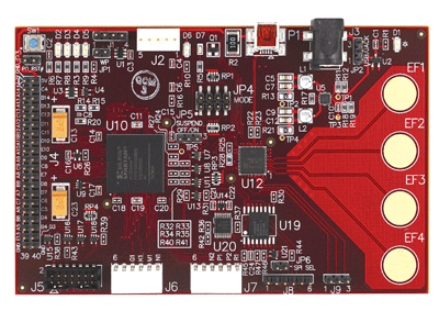
Evaluation kits, such as the $39 Xilinx Spartan-3A from Avnet Electronics for applications based on Xilinx Spartan-3A FPGAs, provide an easy-to-use low-cost platform for designers to experiment and prototype logic designs based on a targeted FPGA family. The $39 Xilinx Spartan-3A eEvaluation kKit from Avnet Electronics provides an easy- to- use, low- cost platform for experimenting and prototyping applications based on the Xilinx Spartan-3A FPGA family.
The evaluation board contained in the kit is populated by a targeted FPGA and fully integrated hardware designed to support and explore the various configuration features of the specific device. Development tools create a user-friendly environment so designers can get an understanding of basic design flow and programming control.
The kits jump-start FPGA designs by providing a pre-engineered, ready-to-use platform allowing designers to immediately begin work on their own logic design goals. They also serve as a hands-on learning tool, teaching a wide range of designers about certain aspects and details of FPGA design. This allows designers to expand their use of FPGA technology and provide product differentiation in a quicker design cycle.
Keeping up with FPGAs
FPGAs continue to revolutionize the way system designers implement logic. With unprecedented increases in logic density and bandwidth, these devices offer an enormous level of design flexibility and performance, allowing them to be used in almost any logic design application. This has prompted the mass migration of logic hardware to the programmable domain, which has transformed how hardware is developed.
The technology is setting new standards for viable and cost-effective logic design, eclipsing traditional fixed-logic ASICs and ASSPs. The reconfigurability of the FPGA platform allows designers to easily program changes or upgrade designs in the field, increasing the life cycle of the end product and eliminating the need for costly hardware redesign and/or ASIC respin.
FPGAs continue to evolve rapidly since first being used as simple “glue logic” devices. They are now key system level components that come with embedded hard and soft core processors, reusable IP cores, block RAM memory, complete clock management, sophisticated I/O capabilities, hard wired multipliers, dedicated peripherals, and advanced DSP functions.
Future growth is ensured by increasing demands in emerging markets for scalable platforms and embedded system development. New devices are being developed every 18 to 24 months with numerous add-ons and feature upgrades appearing along the way.
Making it easier
To keep up with the frenzied pace of innovation where design cycles may last only a few months, designers are pressured to bring products to market quickly and efficiently while keeping development costs down. This can be intimidating for designers sitting in their labs facing the prospect of exploring a new design from scratch with a blank chip and an empty breadboard. It means developing a hardware platform, writing the software code to make it work, then debugging the system to verify its stability. That’s a lot of engineering resources to expend before even looking at the target design.
Designers can significantly reduce the difficulties of this critical first step by using an evaluation kit to get them started. These kits empower the design process by providing a ready-made starting point for designers to quickly initiate their own product development. They range from entry level to advanced, benefiting designers of all experience levels.
Kits can be chosen among available packages by first picking an FPGA supplier and determining a device family that meets design requirements in terms of logic density, clock speed, I/O, and general features. With the complexity of FPGAs, designers should stick with their basic needs when choosing a kit. They can first learn about the technology and then upgrade to a more advanced platform as they become familiar with their particular device and design tools.
Functionally, kits are measured by their ability to demonstrate, evaluate, or develop a component or technology. The degree to which they perform one or more of these functions will vary by board and supplier. Demonstration-orientated kits verify performance specs so engineers can see firsthand that a device conforms to the data sheets. Evaluation kits are used for experimentation, prototyping, and first-stage development. Development kits are used for more-comprehensive advanced designs tailored toward specific applications.
Available hardware
A kit’s evaluation board provides a working, stable platform from which to showcase the FPGA’s configuration and performance features. The integrated hardware contains a mix of support circuitry to operate the system, interface capability to communicate with external devices, and key components to exploit the FPGA’s power.
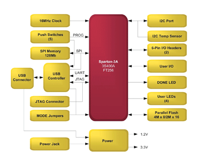
Common hardware features include clocks, status LEDs, control switches, user I/O headers, a JTAG debug interface, a serial communication interface, and power management circuitry. Many boards include nonvolatile flash memory, which can be used to store FPGA configurations, programming code, and data files.

The diversity of the Xilinx Spartan-3A eEvaluation kKit from Avnet Electronics gives designers the ability to explore general FPGA prototyping, MicroBlaze systems, configuration development, USB- powered control, and Cypress PSoC evaluation.
The basic functionality and complexity of the hardware varies by its unique integration of the FPGA with other featured components allowing designers to investigate the latest innovations. For example, the new Xilinx Spartan-3A evaluation kit from Avnet Electronics Marketing (www.em.avnet.com/spartan3a-evl) uses a Cypress PSoC mixed-signal array as a companion chip to the FPGA. This programmable system-on-chip device integrates a microcontroller with the analog and digital components that surround it in an embedded system. Avnet’s kit preconfigures the PSoC to enable direct programming of the FPGA and on-board flash memory through Windows-based software, allowing designers to easily examine a slave serial configuration with an external processor.
As designers gain experience or advance their prototype designs, they can take advantage of connections for expansion boards or modules. These modules provide increased functionality and access to more targeted designs, eliminating the need to jump to more advanced kits until they are ready.
Software tools
The design software that comes with evaluation kits is typically a truncated version of the FPGA supplier’s full-blown development software and is supplied at little or no cost with the kit. But don’t be fooled, these software packages are fully functional and offer designers full immersion into the programmable logic design environment from project start to finish.
The powerful software provides numerous built-in design tools and features, employing a graphical system design approach that makes programming easy and intuitive. Design functions include HDL editors, synthesis, simulation, implementation tools, JTAG programming, board-level integration, device fitting, and verification. Advanced software add-ons are usually offered separately for specialized design needs such as DSP or embedded-systems development.
The design software is typically supported on Windows- or Linux-based systems. Installation is from a supplied DVD or downloadable from the FPGA supplier’s Web site where users can also download upgrades, get the latest reference designs for their chosen kit, or get in touch with technical support if they have any questions.
Exclusive to the FPGA supplier, the design software can typically program all the devices in supported FPGA families contained in the supplier’s product line. This gives designers the advantage of using the same software tools to explore design using different chipsets or when advancing to more comprehensive evaluation kits, reducing the learning curve and saving on development time. ■
Visit fpgadesigns.electronicproducts.com for more information on FPGA design. Xilinx has asserted a considerable market leadership position. They secured over 50% of the PLD market share: larger than all other public PLD companies combined. For more information on Xilinx, visit http://www.xilinx.com. Visit http://fpgadesigns.electronicproducts.com to see full coverage of FPGA designsSponsored by Xilinx • www.xilinx.com
Advertisement
Learn more about Xilinx


