Evolution of MEMS toward a semiconductor model
CMOS-MEMS integration is rapidly becoming a necessity rather than an option for current high-volume MEMS products
BY MIKE DANEMAN, MARTIN LIM, and FARI ASSADERAGHI
InvenSense
www.invensense.com
Almost since the inception of MEMS, the idea of integrating MEMS devices with CMOS circuits has been a grand goal and a subject of much discussion in the industry. In fact, one of the driving forces behind development of surface micro-machining in the late 1980s and early 1990s was the largely unfulfilled promise of compatibility with CMOS processes.
The benefits of CMOS-MEMS integration are many greater functionality in a smaller size, significantly improved testability, lower interconnect parasitics, better shielding, and lower packaging cost. However, while the CMOS industry has continued to make rapid advances in device size and functionality through integration, MEMS devices overwhelmingly remain a two-chip solution with separate MEMS and CMOS die. For designers, it is important to understand the reasons for this discrepancy and the advances that are moving the MEMS industry to a truly integrated model.
Why integrate?
Before discussing the challenges of CMOS-MEMS integration, let us review the driving forces behind it. At the inception of MEMS in the 1970s, most MEMS devices were relatively simple single pressure sensors or large mass accelerometers for industrial applications where the signals could be easily processed with off-chip electronics; extreme size reduction was not a concern.
However, as MEMS evolved into smaller and more complex devices, driven in large part by the consumer electronics market, using external electronics became much less practical. Smaller MEMS devices with weaker and more parasitic-sensitive signals, as well as smaller package requirements, force the CMOS to be closely and compactly coupled to the MEMS.
At the same time, the emergence of larger MEMS arrays, such as mirror arrays for displays or optical telecommunications as well as multi-axis inertial sensor devices, requires integrated electronics to avoid unwieldy MEMS routing and associated parasitics and crosstalk. Furthermore, integrated devices significantly simplify and improve testing, enabling a CMOS-like test flow and device traceability, further reducing cost and improving reliability.
Challenges of integration
CMOS technology has evolved significantly over time from the initial simple transistor process, now offering many process options for integrating additional devices such as RF circuits, OTP, or flash. However, MEMS has generally eluded integration into a CMOS process. There are a few reasons for this. MEMS processes tend to be quite different from a typical CMOS flow, requiring thick layers, high temperatures, and, finally, a release process that undercuts sacrificial layers to allow the MEMS devices to move.
The interaction of CMOS and MEMS processes often compromises both, resulting in a negative impact on yield. Alternatively, using standard CMOS metal and oxide layers for MEMS structures, while more compatible with standard CMOS processes, results in suboptimal mechanical structures in which stress, flatness, and material stability are difficult to control.
In the following sections, we’ll examine the three major approaches to fabrication of MEMS-based components that are being employed today: two-chip, single-wafer, and wafer-level bonding.
Two-chip approach
Most of the MEMS devices in volume production today still use the two-chip solution to interconnect MEMS and CMOS. In this approach, CMOS and MEMS are located in the same package either side by side or stacked on top of each other — and interconnected via wire-bonding (see Fig. 1 ). This is commonly referred to as package-level integration.
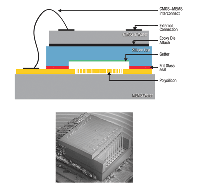
Fig. 1: For a typical two-chip package integration, a CMOS die is bonded on top of a MEMS die and interconnected via wire-bonds.
While this approach has the advantage of fully decoupling the MEMS and CMOS processes and yields, it has a number of downsides. For one, the need for two chips limits how small the package can be, and typically requires a land grid array (LGA) package rather than the less-expensive quad flat no-lead (QFN) package.
In addition, the exposed bond wires act as antennae for electromagnetic interference and must be shielded with a grounded metal lid, further increasing package expense. The wire-bond interconnect and the corresponding bond pads increase parasitic impedance between the chips, limiting ability to sense small signal levels from the MEMS. Finally, the inability to fully test at the wafer level increases test cost and can negatively impact reliability.
While package-level integration is still the most common approach, it is beginning to run out of stream in achieving the smallest, lowest-cost, and highest-performing devices.
Single-wafer integration
The emergence of surface micromachining was largely driven by its promise to integrate MEMS directly with CMOS processes. Using polycrystalline silicon, oxide, and nitride layers, followed by a sacrificial oxide release, MEMS could be built up on top of or next to CMOS on the same wafer (see Fig. 2 ).
Fig. 2. Above are two examples of surface micro-machined structures. Analog Devices’ integrated accelerometer is shown on the left, with the MEMS device in the center surrounded by digital circuitry, and on the right, is a gimbaled micro-mirror for an optical switch with digital circuits beneath.
However, there were significant challenges in integrating the two processes. Using a CMOS-first approach, the choice of materials and processes for MEMS was severely limited due to their effect on CMOS diffusion and metallization layers. While some creative approaches to solve this issue were evaluated, for example by replacing aluminum metallization layers with tungsten, none were incorporated into production due to their impact on the CMOS process.
Another approach fabricating MEMS first and then CMOS had the disadvantage of taking significant area away from the CMOS circuits, since no circuit could be fabricated on top of the MEMS, and required a deep trench for the MEMS that had to be planarized prior to CMOS fabrication. Analog Devices achieved some success in the inertial sensor market with a more integrated approach where CMOS and MEMS process steps were intermixed to achieve true integration. However, the CMOS process was very specific to MEMS and was a significant deviation from a standard CMOS flow. It has, therefore, remained essentially a single-vendor captive process.
More recent approaches have used standard CMOS layers to form MEMS on top of a largely standard CMOS wafer. This is accomplished by using a combination of CMOS metal and inter-metal dielectric layers to form the MEMS structure. This approach achieved some success for some device types (such as microphones and tunable capacitors). However, the design space and reliability are limited by the poor flatness, stress control, and stability of these layers, and significant design complexity is often required to reduce (but typically not eliminate) these issues.
Wafer-level bonding
An alternative approach to CMOS-MEMS integration is wafer-level bonding, such as the process developed by InvenSense as part of the proprietary Nasiri-Fabrication (NF) Platform. In this wafer-level integration approach, a fully processed CMOS wafer is bonded to a fully processed MEMS wafer.
For the NF Platform, this is done using a patented aluminum-germanium eutectic bond (see Fig 3 ). The bond electrically interconnects the two wafers while simultaneously forming a hermetic seal around each MEMS structure.
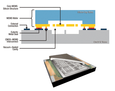
Fig 3: With InvenSense’s wafer-level bonding integrated MEMS structure, MEMS and CMOS combined and inter-connected at wafer-level.
Since wafer-level bonding allows each wafer to be processed separately, an optimal process may be used for each without the compromises required by single-wafer integration. Furthermore, no additional capping wafer is needed to seal the MEMS, since the CMOS wafer acts as a “cap”.
Unlike the single-wafer approaches described previously, the MEMS structure may be bonded directly on top of CMOS circuits preserving valuable CMOS real-estate and allowing MEMS connections to be fully shielded by the CMOS metals. The ability to wafer-level test full devices and eliminate failing parts prior to packaging reduces test cost and improves reliability.
While the total yield of a bonded wafer is determined by both the CMOS and MEMS yields, neither process compromises the other. With typical CMOS yields of 97% to 99%, the overall yield is primarily determined by the MEMS wafer, producing yields on par with the two-chip approach. In addition, integrated CMOS can compensate and trim out many MEMS process variations, further increasing yield and design flexibility. InvenSense has been very successful in using this wafer-level integration process to ship high volume inertial sensors for the consumer electronics market.
To encourage more widespread CMOS-MEMS integration and faster development cycles in the MEMS industry, InvenSense recently opened its NF Platform to outside industrial and academic users as a multiproject shuttle service (NF-Shuttle).
Wafer-level integration, process standardization, and the associated shift to a CMOS-like production and test flow, promises to revolutionize the MEMS industry, making fabless MEMS development as accessible and commonplace as its CMOS counterpart. ■
Advertisement
Learn more about InvenSense


