Extreme makeover for high-temperature converters
Meeting the converter requirements of mil/aero apps requires proper component and material selection, and assembly design
BY TIVA BUSSARAKONSI
nternational Rectifier
El Segundo, CA
http://www.irf.com
Factors such as component characteristics, materials selection, topology, and assembly are all important when it comes to delivering dc/dc conversion technologies that meet the requirements of defense and aerospace applications.
Pushing the boundaries of performance is not always about the search for more MIPS, greater energy efficiency, and smaller size. For military and aerospace designers in particular, advancement is just as often about eliminating failures, increasing safety, designing in longer-term reliability and ensuring resistance to extreme environmental conditions.
By these measures, materials and manufacturing processes are often every bit as important as electronic components themselves particularly when it comes to attaining exacting environmental specifications.
Recent advances in these areas have laid the groundwork for the development of new generations of power conversion products that promise to substantially exceed the performance of existing commercial-off-the-shelf (COTS) alternatives, particularly in the area of high-temperature operation.
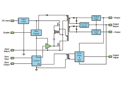
Extreme environmentsUntil recently, dc/dc converters for extreme-high-temperature environments (over 150C) were not readily available off the shelf. In fact, few commercial products could exceed 125C, and none was available beyond 175C. Designers seeking to satisfy the utmost temperature and vibration requirements, such as those encountered in aircraft-engine-control and oil-drilling applications, therefore have typically needed to build their own converters, with consequently long lead-times and substantial non-recurring engineering (NRE) costs.TopologyFigure 1 shows the block diagram of a dual-output dc/dc converter design based around a single-ended forward topology with resonant reset.

Fig. 1. Block diagram of high-reliability dc/dc converter topology.
Working with a nominal switching frequency of 500 kHz and optimized to deliver high-reliability operation at high temperatures, the design uses two high-voltage power MOSFETs in series to accommodate high input voltages while minimizing voltage stress.
In this design, input/output isolation and excellent output voltage regulation are achieved through the use of magnetically coupled feedback. Voltage feed-forward with duty factor limiting provides high line rejection and protection against output overvoltage in the event of an internal control loop failure.
As the diagram shows, the design also includes an LC input filter to control the conducted emission propagating back on to the input lines. In this way, the typical input ripple current can be limited to less than 15 mA peak to peak.
On the output side, two isolated windings with the traditional rectification arrangement are followed by individual low-pass output filters that attenuate the higher-frequency ripple and noise. The built-in output overload and short-circuit protection makes use of the resistance of the inductor wire to reduce power losses. Output voltage is sensed and the control loop is closed across the positive output. The negative output is expected to provide regulation with balanced loads. For a single-output design, only a single secondary winding, associated rectification, and filter circuitry would be required.
Device selectionSo we have a basic topology that we know will meet the performance and functionality we might expect in many high-reliability applications. However, for the converter designer this is only one part of the story. In addition to topological choices, device selection is also important.
In particular, we must look at delivering an electrical design that conservatively derates electrical components if we are to minimize stress and ensure that the completed product functions well within the required parameters. This approach ensures that the design does not require derating with increasing temperature.
Assembly and packagingAssembly and physical design are just as important as circuit topology and device selection when it comes to delivering high reliability. Using a hermetically sealed thick film hybrid package, for example, can help to ensure the lowest possible junction thermal impedances.
A hybrid approach provides an inherent isothermal plane, offering the shortest thermal paths from the components to the base for cooling. By combining this type of packaging with the use of high thermal conductivity materials throughout the design can play a key role in delivering the best possible thermal performance.
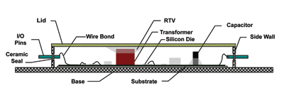
As an example, consider the assembly of an International Rectifier HTA converter, a device specifically designed for high-reliability applications. A cross-section of an HTA device is shown in Fig. 2 . In this case the package comprising base and side wall is a uni-body construction and the package material is aluminum-silicon, which has been chosen because of its excellent thermal conductivity and mechanical robustness.

Fig. 2. Basic cross-sectional view of a dc/dc converter assembly.
The assembly process itself is also vital. This begins with attachment of electrical components by solder reflow or adhesive epoxy to bare beryllium oxide (BeO) thick-film substrates with screen-printed resistors.
Transformers and other magnetic parts are attached to the substrates and base of the assembly with thermally conductive epoxy. The assembled substrates are then solder reflowed to the base. Lead frames and wire bonds are attached from substrate to substrate and from the substrates to the I/O pins.
When the electrical interconnections are complete, the assembly will need to be inspected for manufacturing defects and tested to ensure proper functionality. High-profile components should then be secured with silicone-based gap filler to enhance mechanical stability, and guarantee the requisite shock and vibration performance. The lid is laser sealed to complete the assembly, which should then be retested for function, and subjected to reliability screening.
Qualification testingQualification testing is the last piece of the jigsaw and an important element of the process. Such testing should include an operating life test at high temperatures, extending to device destruction or at least a minimum of 10,000 hours.
Temperature cycling and shock testing will also be required, while vibration resistance will be measured by subjecting devices to full load operation under a variety of vibration frequencies. Not only should these tests show that the design performs within specification but, equally important, they need to demonstrate as little variation from device to device as possible a key criterion for users looking to reliably characterize the converters’ expected operation.
Value-added featuresConservative design disciplines, well characterized performance and COTS availability all contribute to dc/dc conversion technologies that will address the performance, reliability, and commercial requirements of military and aerospace OEMs.
However, in order to optimize the familiar COTS advantages of reduced NRE and faster time to market, it will often be necessary to design-in a number of value-added features. The HTA dc/dc converters mentioned previously, for example, include the ability to synchronize multiple converters and thus service higher power requirements precise output adjustment and on/off control. Single-output models include remote output sensing, and the galvanic isolation between input and output not only allows several converters to be stacked to deliver higher voltages, it also protects the output load from input-side system failures. ■
For more on dc/dc converters, visit http://www2.electronicproducts.com/Power.aspx
Advertisement
Learn more about International Rectifier


