MICHELLE LI, systems engineering manager,
and SAMUEL WONG, systems engineer,
Texas Instruments,
www.ti.com
As the functions of portable devices increase, the need for more battery capacity continues to grow. Larger batteries can mean longer charge time, but users also demand less charge time or the ability to charge the battery more fully within the same amount of time. To meet this stringent requirement, the charge current must be increased significantly. A traditional 5V USB adapter with limited input power can no longer satisfy this fast-charging demand.
Industry initiatives to support higher adapter power such as USB Type-C and other methods to provide USB-compatible, high-voltage input are becoming more popular. As system designers try to take full advantage of new high-voltage adapters, they are faced with new challenges. These include how to improve charging efficiency with minimum cost impact, how to break the thermal loss barrier, and how to minimize the impact of battery path impedance with much higher charging currents. In this article we discuss these challenges and provide possible design solutions.
Smartphone functions have become indispensable tools in our daily life. To deliver increased data processing power, power-hungry processors are needed to deliver this breakthrough performance. However, processor power consumption has not scaled with the CPU processor. Therefore, higher capacity batteries are needed so that the device can match CPU processing power. Using the same input power and charging system, doubling battery capacity requires doubling the charge time. For example, a typical two-hour charge time will be doubled to four hours or longer. Clearly this scaling is not acceptable in many applications.
USB power limitations
To design a high-power charging system, designers have to provide sufficient input power. Using simple physics (power = voltage x current), designers can choose to increase the current or the input source voltage. Traditionally, system designers need to increase the current of the 5V USB power source in order to meet the demand for higher charging power. For example, USB 2.0 can provide a maximum output current of 500 mA, USB3.0 can provide up to 900 mA, and a USB dedicated charging port (DCP) based on the battery charging BC1.2 standard can provide up to 1.5A output current. Current USB Type-C connectors can support up to 3A of output current.
However, this approach is coming to an end. Several limitations are preventing designers from further increasing output current:
1. USB connectors are typically rated for 1.8A, unless it is custom-designed or uses USB Type-C 3A connectors. However, higher current is often associated with higher connector cost.
2. USB cables generally have about 150-300 mΩ cable impedance, depending on quality. When cable IR drop is taken into account with 2A current, the 5V output can be lowered to 4.4V. Unfortunately, not enough headroom is left to charge an advanced Lithium-Ion (Li-Ion) battery of 4.35V or higher.
Based on these limitations, if designers want to meet the challenge of providing sufficient power for battery charging, designers need to increase the input voltage,.
Breaking the USB power barrier
To achieve 1C charging for a 4-AHr battery with 90 percent efficiency, a simple back-envelop calculation shows that 16.8W of power is needed (3.8V x 4A / 0.9). Given a typical 2A adapter rating, an 8.4V or above adapter output voltage is required. This concept is similar to that of a utility power system that uses a high-voltage grid to deliver power from the generators to end users, providing high power with less loss.
To be backwards-compatible with a traditional 5V USB adapter, new adjustable high-voltage adapters are available to support, for example, 9V/2A and 12V/1.5A outputs. When first plugged-in, the adapter delivers 5V output similar to traditional USB adapters. The system communicates with the adapter through various methods to increase output voltage up to 7V, 9V or 12V. The adapter continues to supply high voltage when output current is drawn.
When the system is un-plugged or under light-load conditions, the adapter is reset to 5V. This ensures system safety when the adapter is plugged-in to other portable equipment. Several proprietary handshakes between the system and adapters have been proposed, based on the input current pulse or D+/D– voltage/current source. Additionally, the USB power delivery standard aims to increase the power level from existing USB standards up to 100W.
Adjustable high-voltage adapters challenge older system designs with constant 5V output voltage. The system must monitor the adjustable input voltage to maintain safety. For example, most systems use an analog-to-digital converter (ADC) to monitor voltage. However, since most ADCs are designed for low-voltage applications, such as 5V or 3V inputs, a voltage divider is needed to divide down the high voltage in order to operate the ADC below its maximum rating. Furthermore, when the ADC input is connected to the USB connector, which is exposed to the external environment, system designers need to pay special attention to possible higher electrostatic discharge (ESD) rating requirements.
Fast-charging challenges
A high-power adapter is the first step to achieving fast charging. With high-input power, the power loss inside a system is increased, which can heat up portable equipment. Typically, the case temperature of a portable device should not exceed 20°C. End users often feel uncomfortable when temperatures rise is beyond this limit. The elevated temperature can also create a unsafe operating environment for the battery, which requires the charging environment to be less than 60°C. To achieve fast and cool charging, systems require a highly efficient way to convert the input power along with methods to control the case temperature while achieving the highest-charging current possible.
Figure 1 shows the topology of a step-down, switch-mode charging system. A MOSFET Q1 is the reverse-blocking FET, and BATFET Q4 is used as the battery-charging control FET. In many applications, Q1 and Q4 are integrated into a charger IC and also serve as input current sense and battery-charging current sense components.
MOSFET Q2, Q3, L, and C comprise the core of a step-down buck converter. Losses of a buck converter consist of conduction and switching losses. At high-output current, conduction loss dominates and can be estimated as:
PLOSS = PLOSS_Q2 + PLOSS_Q3 (1)
PLOSS_Q2 = ICHG 2 x RDS_Q2 x D (2)
PLOSS_Q3 = ICHG 2 x RDS_Q3 x (1-D) (3)
Where D = VOUT / VIN (4)
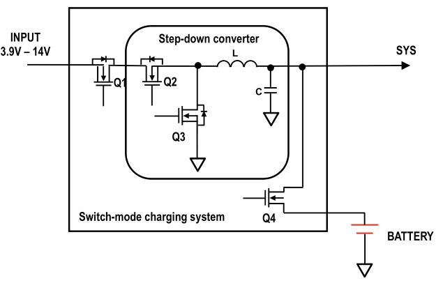
Fig. 1: An illustration of the topology of a step-down buck converter charging system
For traditional 5V input, the duty cycle (D) is about 80 percent for 4V output. This implies that RDS_Q2 is the dominant loss element. For new high-voltage input such as 12V, the duty cycle is about 33 percent for 4V output. RDS_Q3 becomes the dominant loss element. System cost is inversely proportional to RDS. For example, the lower the RDS , the higher the transistor cost. For high-voltage input such as 9V/12V, it is more effective to scale RDS_Q3 lower for a low-duty cycle converter.
In addition to supplying the charging current, the buck converter can provide power to the system load while users run their applications. Graphic-intensive gaming applications can demand very high system power and become the hottest spot inside the portable device. To further complement the highly efficient buck converter, a thermal regulation loop is desirable. A thermal regulation loop can maintain the IC junction temperature below a predefined threshold by reducing the charge current. Figure 2 shows how a charger with thermal regulation can help to maintain the IC junction temperature around 80°C and 120°C.
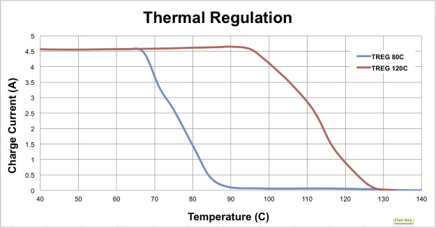
Fig. 2: The effect of a thermal-regulated charge current versus an IC junction-based temperature
The standard method to charge a Li-Ion battery consists of constant current-mode, followed by constant voltage-mode. Constant current-mode represents the highest current when a battery is being charged. For fast-charging, it is best to keep battery-charging in the constant current-mode as long as possible. Figure 3 shows several system components in the charging path including PCB trace, battery connectors, protection MOSFETs, and a sense resistor that can affect the charge time.
With high-charge current, the effect of charging path resistance is significant. The voltage drop across the resistance can force the charging process to transition from constant-current to constant-voltage early, and extends the charge time. To alleviate this challenge, system designers need to use higher quality components, such as lower RDSON MOSFETs and improved connectors – which also involves higher costs.
Alternatively, a charging system can compensate for the IR drop by lifting the charging voltage output at the charger adaptively. This is based on the charge current while keeping the voltage at the battery terminal within its recommended charge voltage limit. Using the IR compensation method, a system can extend the constant current-mode during battery charging without adding cost.
Figure 3 shows how the charging time speeds up when using the IR compensation technique. Charge time improves by 17 percent from 234 to 200 minutes when the 70 mΩ path resistance is compensated.
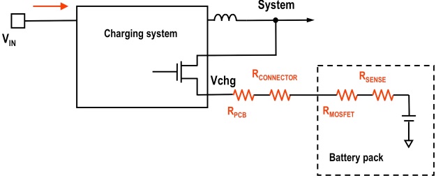
Fig. 3: Example of a typical charging path resistance
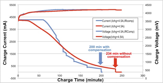
Fig. 4: Charge time comparison between one system with compensation and one without
With the increase of battery capacity, fast charging is becoming a must-have feature in many portable applications. To meet the challenge, more input power is required, which is accomplished by deploying adjustable high-voltage adapters. In order to utilize the input power effectively, a highly efficient step-down converter is required, with careful consideration given to the duty cycle effect. Finally, other techniques such as thermal regulation and resistance compensation are necessary in order to maximize the benefit of high charging current while providing an improved end user charging experience.
References
- More information about battery charge management.
- Download the bq25892 datasheet.
Advertisement
Learn more about Texas Instruments


