Ferroelectric nanotubes for THz emitters, energy harvesters
Researchers at Georgia Institute of Technology have developed a “soft template infiltration” technique for fabricating free-standing piezoelectrically active ferroelectric nanotubes and other nanostructures from PZT (lead zirconate titanate). This is important because PZT has a large piezoelectric response. The technique allows fabrication of ferroelectric nanostructures with user-defined shapes, location and pattern variation across the same substrate.

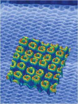
Composite scanning electron microscope image of PZT nanotube arrays and their piezoelectric response as measured by band-excitation PFM. (Image courtesy of Ashley Bernal and Nazanin Bassiri-Gharb.)
The resulting structures have a 100 to 200-nm outer diameter with thickness ranging from 5 to 25 nm, and show a piezoelectric response comparable to that of PZT thin films of much larger dimensions. The technique could ultimately lead to production of actively-tunable photonic and phononic crystals, terahertz emitters, energy harvesters, micromotors, micropumps and nanoelectromechanical sensors, actuators and transducers — all made from the PZT material.
Ferroelectric materials at the nanometer scale are promising for a wide range of applications, but processing them into useful devices has proven challenging — despite success at producing such devices at the micrometer scale. Top-down manufacturing techniques, such as focused-ion-beam milling, allow accurate definition of devices at the nanometer scale, but the process can induce surface damage that degrades the ferroelectric and piezoelectric properties that make the material interesting.
Until now, bottom-up fabrication techniques have been unable to produce structures with both high aspect ratios and precise control over location. The technique reported by the Georgia Tech researchers allows production of nanotubes made from PZT (PbZr0.52Ti0.48O3) with aspect ratios of up to 5 to 1.
The ferroelectric nanotubes are especially interesting because their properties — including size, shape, optical responses and dielectric characteristics — can be controlled by external forces even after they are fabricated. They can be tuned to behave differently from each other.
For example, the piezoelectric effect could permit fabrication of “nano-muscle” tubes that would act as tiny pumps when an electric field is applied to them. The fields could also be used to tune the properties of photonic crystals, or to create structures whose size can be altered slightly to absorb electromagnetic energy of different wavelengths.
The piezoelectric nanomaterials will help generate a factor of four to six increase in the extrinsic piezoelectric response compared to the use of thin films, and that will lead to the use of smaller structures than are currently used today.
Though the researchers used electron beam lithography to create the template on which the structures were grown, in principle, many other chemical, optical or mechanical patterning techniques could be used for create the templates, according to Bassiri-Gharb. For more information go to http://gtresearchnews.gatech.edu/ferroelectric-piezoelectric-nanotubes/.
Paul O’Shea
Advertisement
Learn more about Electronic Products Magazine


