By Majeed Ahmad, contributing writer
Achronix Semiconductor Corp. claims that its Speedster7t family of FPGAs designed for artificial intelligence (AI), machine learning (ML), and other high-bandwidth workloads offers ASIC-like performance while ensuring FPGA adaptability. Achronix calls it “FPGA+,” as it blends FPGA programmability with ASIC routing structures and compute engines.
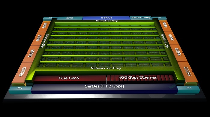
The Speedster7t FPGAs, manufactured on TSMC’s 7-nm FinFET process, feature a 2D network-on-chip (NoC) and a high-density array of new machine-learning processors (MLPs). It also features high-bandwidth GDDR6 interfaces, 400G Ethernet ports, and PCI Express Gen5, and they are all interconnected to deliver ASIC-level bandwidth while retaining the full programmability of FPGAs.
Achronix said that the Speedster7t devices are the only FPGAs that support GDDR6 memory devices. Each GDDR6 memory controller is capable of supporting 512 Gbits/s of bandwidth, and the up to eight GDDR6 controllers in a Speedster7t device can support an aggregate GDDR6 bandwidth of 4 Tbits/s, which delivers the equivalent memory bandwidth of an HBM-based FPGA at a fraction of the cost, said the company.
According to Achronix, its engineering team has redesigned the entire FPGA architecture to balance on-chip processing, interconnects, and external I/O so that designers can maximize the throughput of data-intensive workloads like those found in edge- and server-based AI and ML applications in networking and storage realms.

The new FPGAs aim to eliminate bottlenecks and ensure the free flow of data in AI and ML applications. The devices are designed to accept massive amounts of data from multiple high-speed sources, distribute the data to programmable on-chip algorithmic and processing units, and then deliver the results with the lowest latency, said Achronix.
The FPGAs also provide advanced security with bitstream security features with multiple layers of defense for protecting bitstream secrecy and integrity. Keys are encrypted based on a tamper-resistant physically unclonable function (PUF), while bitstreams are encrypted and authenticated by 256-bit AES-GCM.
For protection from side-channel attacks, bitstreams are segmented, with separately derived keys used for each segment, and the decryption hardware uses differential power analysis (DPA) countermeasures. The FPGAs also use a 2,048-bit RSA public key authentication protocol to activate the decryption and authentication hardware.
The first devices and development boards for evaluation will be available in the fourth quarter of 2019.
Advertisement
Learn more about Electronic Products Magazine


